


-
multi_layer Fiber Sphere Ananth AIN Defect 2d_materials Step Growth NUS_NNI_Nanocore food LightEmission Cross-section Filter TipBiasMode HDD NanoLithography 2dMaterials LowDensityPolyethylene Techcomp Change fifber SSRM MfmAmplitude silicon_oxide Ecoli ScratchMode Terrace PinPointMode PetruPoni_Institute Yeditepe Tape Etch Barium_titanate BCZT
Report image
If you found this image unacceptable, please let us know. We will review your report and take action if we determine this image is really unacceptable.
Multi-layer necking device defect
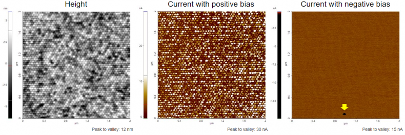
Scanning Conditions
- System : NX-Wafer
- Scan Mode: C-AFM
- Scan Rate : 2Hz
- Scan Size : 2μm×2μm
- Pixel Size : 512×256
- Cantilever : AD-2.8-AS (k=2.8N/m, f=75kHz)