


-
IMT_Bucharest UnivMaryland ThermalProperties HighAspect Phosphide FM_KPFM SiliconeOxide contact ImideMonomer Pattern Typhimurium block_copolymer Melt MfmAmplitude ScanningSpreadingResistanceMicroscopy BismuthVanadate Piranha CaMnO3 Wafer Piezo FAFailureAnlaysis LiquidImaging dielectric_trench VortexCore mfm_amplitude ElectroDeposition Christmas Chemical_Vapor_Deposition temp MoS2 aluminum_nitride FM-KPFM Nanopattern fluorocarbon MultiLayerCeramicCapacitor
Report image
If you found this image unacceptable, please let us know. We will review your report and take action if we determine this image is really unacceptable.
WLI image of wafer ID mark
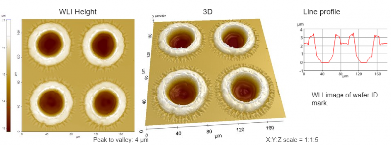
Scanning Conditions
- System : NX-Hybrid WLI
- Scan Mode: WLI
- Field of view: 182μm×182μm