


-
Scanning_Thermal_Microscopy MonoLayer OpticalWaveguides SurfaceChange temperature controller AFM Multiferroic_materials Gold AlkaneFilm strontiu_titanate Regensburg Pipette Trench Monisha Pinpoint PFM small_scan CVD mfm_amplitude CHRYSALIS_INC InorganicCompound heterojunctions Imprint Sadowski Anneal phase_change Metal-organicComplex Photovoltaics PFM mono_layer MfmAmplitude Etch TungstenThinFilmDeposition Polyethylene Barium_titanate Tape DeoxyribonucleicAcid
Report image
If you found this image unacceptable, please let us know. We will review your report and take action if we determine this image is really unacceptable.
Defect of LinbO₃
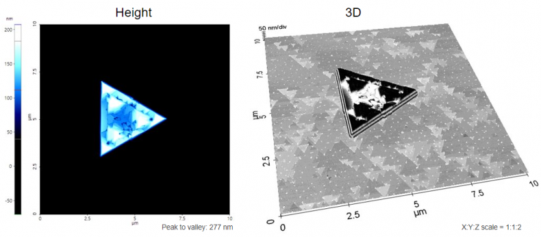
Scanning Conditions
- System : FX40
- Scan Mode: Non-contact
- Scan Rate : 0.3 Hz
- Scan Size : 10μm×10μm
- Pixel Size : 1024×512
- Cantilever : SCOUT 350 (k=42N/m, f=350kHz)