


-
Alkane PrCurve CrossSection SiliconeOxide OpticalWaveguides Piezo Cobalt TiO2 AM-KPFM conductive Materials hard_disk_media layers Tin sulfide CeNSE_IISc Techcomp Indent mono_layer China KPFM electrospinning Ni81Fe19 Hafnia Dopped KelvinProbeForceMicroscopy Lanthanum_aluminate #Materials Praseodymium ito_film Nanopattern MultiLayerCeramicCapacitor Potential hetero_structure LateralPFM piezoelectric force microscopy
Report image
If you found this image unacceptable, please let us know. We will review your report and take action if we determine this image is really unacceptable.
PS/LDPE
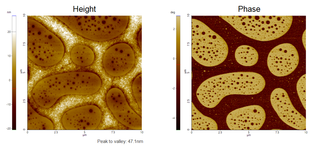
Spincast layer of PS/LDPE blend on Si.
Scanning Conditions
- System: NX20
- Scan Mode: Tapping
- Cantilever: AD40AS (k=40N/m, f=180kHz)
- Scan Size: 10μm×10μm
- Scan Rate: 0.5Hz
- Pixel Size: 512 × 256
- Scan Mode: Tapping
- Cantilever: AD40AS (k=40N/m, f=180kHz)
- Scan Size: 10μm×10μm
- Scan Rate: 0.5Hz
- Pixel Size: 512 × 256