


-
BTO ConductiveAFM semifluorinated alkane semifluorinated_alkanes Self-assembledMonolayer Defect Annealing Hafnium_dioxide Layer Imprint FloppyDisk Oxide Spain Hexatriacontane FailureAnlaysis Platinum FAPbI3 Conductive AFM NCM Polydimethylsiloxane Temperature TiO2 ThermalConductivity INSPParis TransitionMetal Conduct Vac SFAs Ram Al2O3 AnodizedAluminumOxide Indent MoirePattern hard_disk_media LDPE
Report image
If you found this image unacceptable, please let us know. We will review your report and take action if we determine this image is really unacceptable.
Monolayer Graphene on PDMS Surface
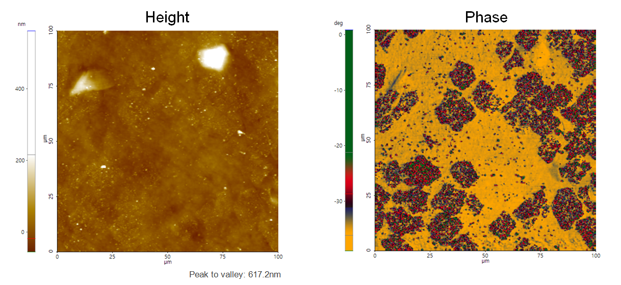
Monolayer Graphene grown on Cu foil using CVD process is transferred on to PDMS substrate.
Scanning Conditions
- System: NX20
- Scan Mode: Tapping
- Cantilever: Access-NC (k=113N/m, f=330kHz)
- Scan Size: 100μm×100μm
- Scan Rate: 0.6Hz
- Pixel Size: 256 × 256
- Scan Mode: Tapping
- Cantilever: Access-NC (k=113N/m, f=330kHz)
- Scan Size: 100μm×100μm
- Scan Rate: 0.6Hz
- Pixel Size: 256 × 256