


-
self_healing SmalScan Display OpticalModulator HexagonalBN Korea Hafnia NiFe Holes BlockCopolymer Techcomp Optoelectonics OpticalElement HardDisk Composite Praseodymium Chemical Vapor Deposition Gallium Metal HanyangUniv Temperature ForceVolumeImage BismuthFerrite Polyethylene Conductivity multi_layer SAM MetalCompound hetero_structure ContactMode Typhimurium dielectric_trench NUSNNI Solution Boundary
Report image
If you found this image unacceptable, please let us know. We will review your report and take action if we determine this image is really unacceptable.
Taegeuk Mark Lithography on PZT
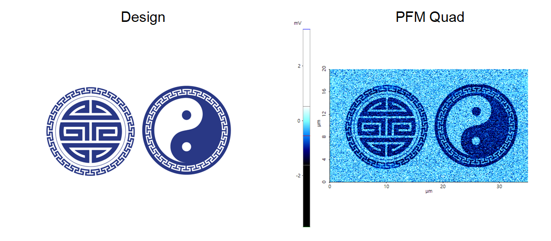
Re-arranged the domain pole direction on PZT surface using bias mode of lithography.
Scanning Conditions
- System: NX10
- Scan Mode: Lithography
- Cantilever: PPP-ContScPt (k=0.2N/m, f=25kHz)
- Scan Size: 35μm×20μm
- Scan Rate: 0.5Hz
- Pixel Size: 1024 × 1024
- Tip Bias: 10V for patterned area
- Scan Mode: Lithography
- Cantilever: PPP-ContScPt (k=0.2N/m, f=25kHz)
- Scan Size: 35μm×20μm
- Scan Rate: 0.5Hz
- Pixel Size: 1024 × 1024
- Tip Bias: 10V for patterned area