


-
tip_bias_mode Galfenol GranadaUniv Multiferroic_materials Tape ShenYang amplitude_modulation semifluorinated_alkane dielectric_trench Indent FAFailureAnlaysis Organic PVAC fluorocarbon multi_layer SmalScan Hafnia LightEmission SurfaceOxidation Optic CP-AFM Varistor exfoliate StainlessSteel ScratchMode FrequencyModulation IRDetector DNA atomic_steps Mapping STM AIN Cell TCS AtomicSteps
Report image
If you found this image unacceptable, please let us know. We will review your report and take action if we determine this image is really unacceptable.
Trench Etch Profile on Si Wafer
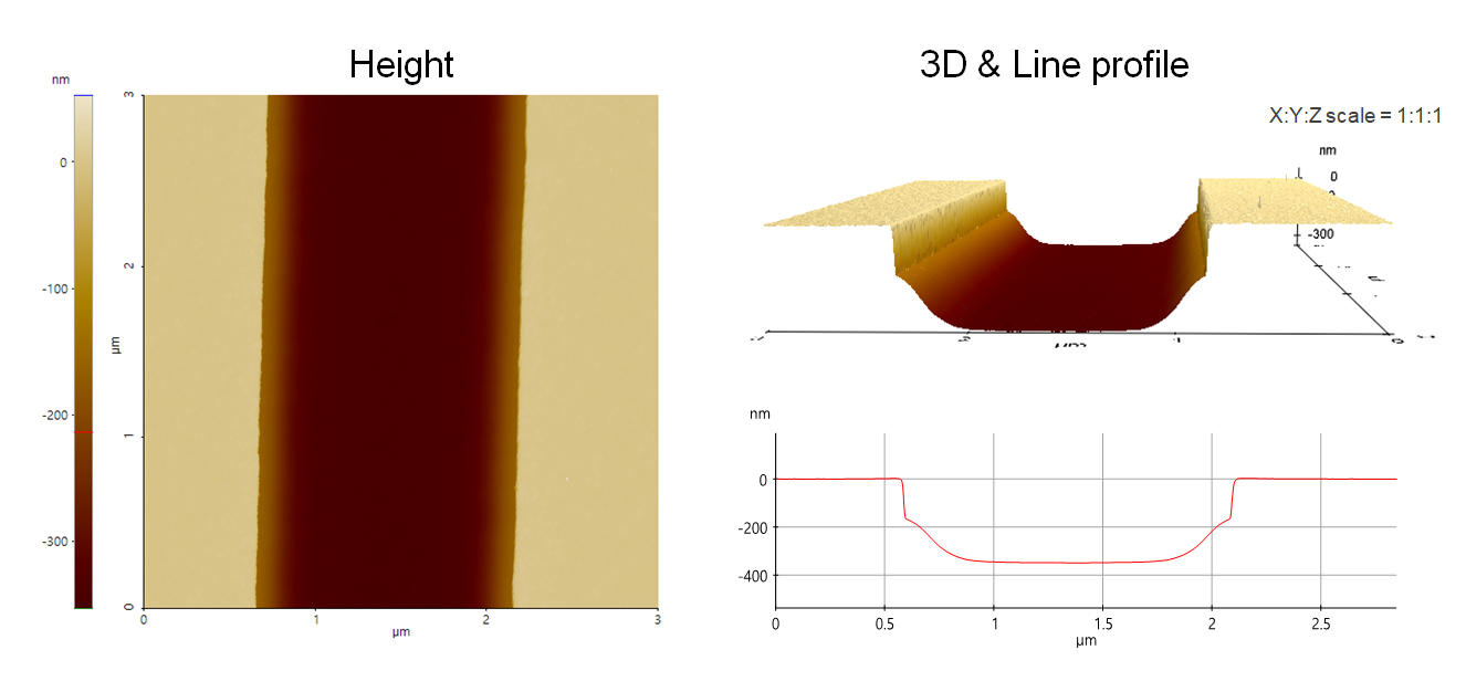
Top dielectric trench etch profile on Si wafer having tapered slope at the trench sidewall.
Scanning Conditions
- System: NX20
- Scan Mode: Non-contact
- Cantilever: AC160TS (k=26N/m, f=300kHz)
- Scan Size: 3μm×3μm
- Scan Rate: 0.21Hz
- Pixel: 1024 × 256
- Scan Mode: Non-contact
- Cantilever: AC160TS (k=26N/m, f=300kHz)
- Scan Size: 3μm×3μm
- Scan Rate: 0.21Hz
- Pixel: 1024 × 256