


-
Inorganic_Compound Electronics Pipette Tungsten Granada Optic polyvinyl acetate STM Kevlar Cell Beads Pvdf ElectroChemical LiquidImaging Formamidinium_lead_iodide YttriaStabilizedZirconia Step TiO2 AIN Sphere fluoroaalkane CarbonNanotube temperature_control Platinum Yeditepe CuSubstrate block_copolymer FM_SKPM Fet molecule PhaseChange H-BN Growth light_emitting Scratch
Report image
If you found this image unacceptable, please let us know. We will review your report and take action if we determine this image is really unacceptable.
AlN/GaN/AlN Hetero Structure
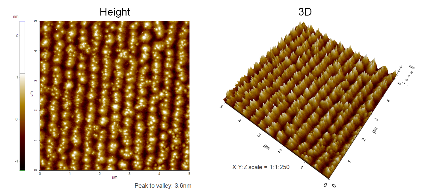
AlN/GaN/AlN hetero structure grown on SiC substrate by Molecular Beam Epitaxy (MBE) system.
Scanning Conditions
- System: NX20
- Scan Mode: Non-contact
- Cantilever: AC160TS (k=26N/m, f=300kHz)
- Scan Size: 5μm×5μm
- Scan Rate: 0.5Hz
- Pixel Size: 512 × 512
- Scan Mode: Non-contact
- Cantilever: AC160TS (k=26N/m, f=300kHz)
- Scan Size: 5μm×5μm
- Scan Rate: 0.5Hz
- Pixel Size: 512 × 512