


-
Croatia MESA structure Phosphide Current Pinpoint PFM Indent HfO2 Electical&Electronics GlassTemperature Polystyrene semifluorinated_alkane Force-distance Polydimethylsiloxane India dichalcogenide BismuthFerrite PANI Neodymium DeflectionOptics Transparent CuParticle PetruPoni_Institute Temperature neodymium_magnets Sio2 Thermoplastic_polyurethane Mobile Sulfur NUS_Physics mechanical_property Oxidation Display InorganicCompound 2-vinylpyridine Device
Report image
If you found this image unacceptable, please let us know. We will review your report and take action if we determine this image is really unacceptable.
ITO Film Sputter Deposited onto Silicon
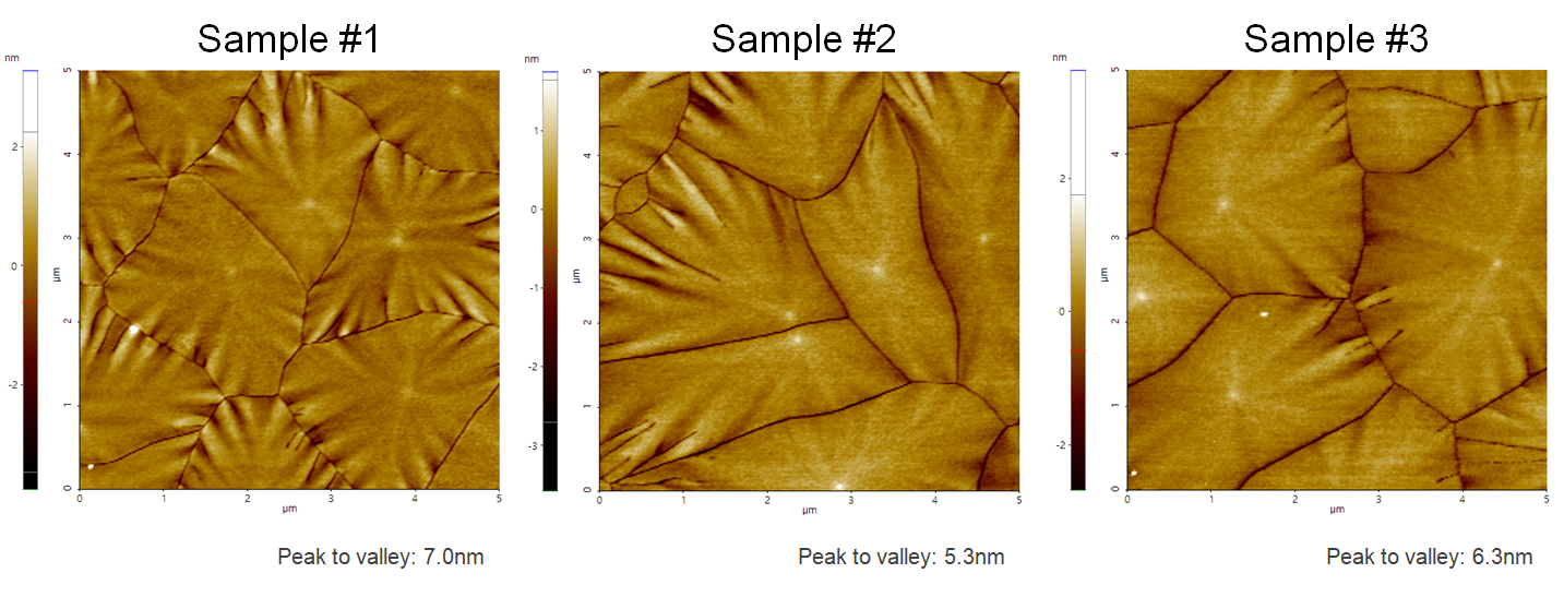
ITO-film, which was sputter deposited onto silicon. The grain size of those samples was influenced by changing the process settings in the Cluterline RAD sputter deposition system, one of the deposition tool platforms manufactured by Evatec.
Scanning Conditions
- System: NX10
- Scan Mode: Non-contact
- Cantilever: PPP-EFM (k=2.8N/m, f=75kHz)
- Scan Size: 5μm×5μm
- Scan Rate: 0.1Hz
- Pixel Size: 256 × 256
- Scan Mode: Non-contact
- Cantilever: PPP-EFM (k=2.8N/m, f=75kHz)
- Scan Size: 5μm×5μm
- Scan Rate: 0.1Hz
- Pixel Size: 256 × 256