


Nano-scale Topography Measurements by AFM: A Note on Repeated Height and Roughness Analyses
Surface properties at the nano-scale
With the evolution of nanotechnology, the need to understand nano-scale and sub nano-scale surface properties is becoming increasingly important. Particularly, surface properties such as topography and roughness play an important role in the overall performance of a material. For example, in integrated circuits manufacturing, chemical mechanical polishing (CMP) has been used to control the surface roughness of wafers and other substrates, which directly determines the reliability of final products [1,2]. In semiconductor devices packaging, wafer to wafer bonding quality is determined by the roughness of bonding surfaces. It was found that surfaces with high roughness values introduce voids in the bonded interface, and bonding failure occurs when the roughness exceeds a critical threshold [3]. In the field of scientific research, surface topography can be correlated with other material properties to better understand material behaviors for practical applications [4–6].
To assess the surface topography of a sample, several methods are available, including stylus profilometry, coherence scanning interferometry, laser microscopy, and atomic force microscopy (AFM). The choice of method depends on the specific characteristics of the sample and the goals of the measurement. In the realm of semiconductor and electronic devices manufacturing, where in-depth insights into nano-scale surface properties are imperative, AFM has been widely used owing to its ability to provide three-dimensional data with sub-nanometer resolution capabilities. In addition, the scanning probe-based methodology of AFM facilitates simultaneous measurements of the surface topography as well as various electrical, frictional, and mechanical properties of the sample, thereby enhancing overall efficiency and throughput.
Measuring the surface properties using AFM
AFM has been widely adopted by industrial chip manufacturers and academic researchers for nano-scale surface measurement of various materials. The AFM can be implemented in in-line and off-line measurements for quality control and inspection of semiconductor and display manufacturing processes. Surface roughness inspection of bare wafers [7], surface roughness measurement after CMP [1,2], wafer bonding process monitoring [3,8], and hard disk media defect inspection and review [7] are typical examples of surface measurements based on AFM. In academic research, surface measurement is related to investigation of nanomaterials [9], correlative study of surface and other material properties [4], or studies of effects of environmental factors on surface properties of material [5,6]. Given that AFM uses a nanoscopic tip to scan the sample surface, it is crucial to understand interactions between the AFM tip and the sample to appropriately analyze and interpret the data. This whitepaper reviews AFM methodologies that are typically used to investigate the topography and roughness of a samples. In particular, AFM data analysis and interpretation procedure, along with related experimental issues will be discussed for an accurate reconstruction of the sample surface.
AFM scan modes to measure the surface
To characterize a surface using the AFM, different scan modes are available such as Contact, Non-contact, and Tapping modes. The scan mode should be selected in consideration of material characteristics and measurement targets. Contact mode was the very first introduced scan mode of AFM that is used to reconstruct the sample surface [10]. Contact mode uses a relatively soft cantilever to raster scan the sample surface. The deflection of the cantilever during scanning provides information on the surface topography. A major drawback of contact mode is exerted shear force during scanning which can cause damage to the tip apex and the sample, especially when scanning soft samples such as polymers and biological materials. To minimize tip and surface damage due to contact scanning, Non-contact mode was developed [11]. In this mode, the tip oscillates in close proximity to the surface in the van der Waal attractive force regime. The oscillation amplitude of the cantilever is used as a feedback signal to keep a constant tip-sample distance. There is no physical contact between the tip and the sample in Non-contact mode, thus facilitating non-invasive and highly accurate topography imaging. However, in certain cases, the sample surface in ambient conditions is covered by an adsorbed fluid layer, whose thickness is larger than the gradient of van der Waals force, affecting the stability and resolution of a non-contact scan. Later on, Tapping mode was introduced [12]. This mode operates in the van der Waal repulsive force regime, where the tip taps the sample surface. As a result, the tip can go through the adsorbed layer and reach the actual sample surface. Also, Tapping mode is more effective for rough and sticky samples. The principles and major applications of each scan mode are summarized in Table 1. The proper scan mode should be selected by considering sample characteristics and target of measurement.
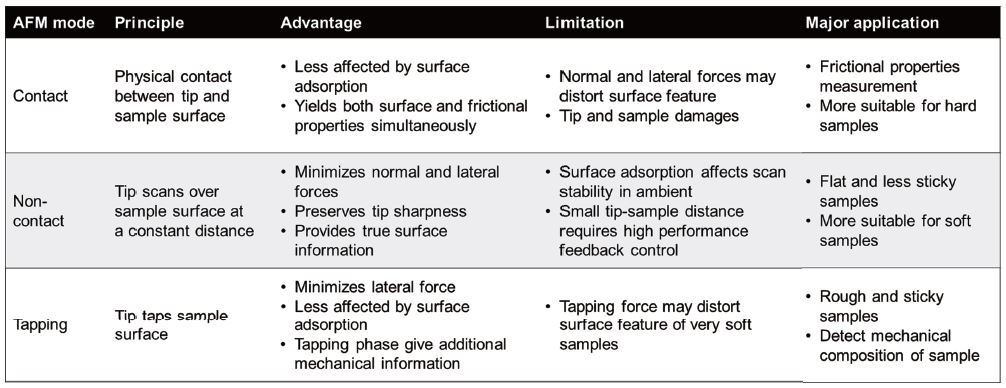
Table 1. Summary of typically used AFM modes to measure the surface.
Park Systems’ solutions for surface measurement
AFM is well-known as a powerful tool for nano-scale metrology. However, AFM data acquisition and analysis procedures are relatively complicated which require long hours of training and practicing. To enhance production throughput and yield, especially in the field of industry, an automated AFM flatform is a key factor. Park Systems offers a variety of hardware and software solutions for both industrial and research applications:
• Fully automated industry AFMs for in-line semiconductor production with customizable recipes for data acquisition and analysis • Research AFMs with user-friendly software, innovative imaging modes and technologies, and batch programmable multiple measurements for advanced scientific research • Various functions designed for throughput enhancement such as automated defect review for industry wafers, narrow trench mode for high aspect ratio structures, FastApproachTM and AdaptiveScanTM to speed up imaging, EZ flattenTM for quick data analysis, etc.
A challenging issue of conventional non-contact measurements is to hold the tip in the attractive force regime. Especially when scanning a rough sample at high speed, the tip may accidentally touch the surface asperity due to the slow response of the Z scanner. Holding a small tip-sample distance requires a high bandwidth Z scanner for fast feedback response. True Non-contactTM scan mode of Park Systems' AFMs offers such performance. The rapid response Z scanner enables a quick movement of the tip in case of an abrupt change in topography, avoiding contact with the sample. In addition, by minimizing the force applied to the tip and sample, true Non-contact mode allows non-invasive characterization of surface properties.
Key considerations for AFM data acquisition and analysis for surface measurement
Although automated AFM solutions are designed to facilitate user convenience, it is important to understand the data acquisition and analysis procedures for a better interpretation of the result. For example, in addition to choosing a proper scan mode, how to select an appropriate scan size, how to flatten the image, or how to select a proper roughness parameter to describe the surface should be taken into consideration.
Selecting the scan size
To properly characterize a surface, the selection of scan size (or cut-off length) is crucial considering that surface properties are dependent on the scale of a measurement. Surface texture typically consists of waviness and roughness [13]. Waviness refers to longer wavelengths on the surface which is related to surface preparation and finishing methods. Roughness refers to fluctuations on shorter wavelengths or irregularities of the surface. Due to the difference in wave amplitude and spacing, the selection of cut-off length directly affects the results of surface roughness calculation.
Fig. 1 presents an example of the effect of scan size on the surface properties of a polystyrene film coated on silicon substrate. The sample surface has a waviness with a spacing of about 80 μm and an amplitude of about 130 nm, as shown in the 3D image and line profile at 100×100 μm2 scan size in Figs. 1(a) and 1(b). The waviness is likely associated with the sample preparation method. A high magnification scan at 5×5 μm2 reveals the surface roughness of the sample, which is characterized by waves with much smaller spacings and amplitudes compare to those of the waviness (e.g., 0.4 μm spacing and 0.45 nm amplitude, as shown in Fig. 1(b)). As a result, the calculated roughness values are significantly different between 100 μm and 5 μm cut-off length scans, as summarized in Fig. 1(c). It should be noted that the cut-off length should be selected depending on the target of a measurement. For example, if the specific application of the material requires an understanding of interfacial properties at a larger contact area, the waviness should be taken into account. In contrast, a smaller cut-off length can be selected to avoid the influence of surface waviness when the surface roughness needs to be studied.
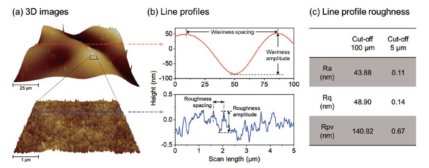
Fig. 1 (a) 3D topography images of a polystyrene film coated on silicon substrate (displayed with low magnification above and zoomed-in view below), (b) cross-sectional line profiles extracted from the red and blue dashed lines in (a), and (c) arithmetic average roughness (Ra), root-mean-square roughness (Rq), and peak-to-valley roughness (Rpv) calculated from line profiles in (b).
Flattening the image
Nano-scale measurement is susceptible to even a small miss-alignment of the sample surface. As demonstrated in Fig. 2(a), the sample surface is tilted, likely due to sample mounting error. This issue occurs in almost every AFM measurement. To level the surface slope, a flattening process is applied to the AFM data. Common approaches to level a surface include plane flattening and line-by-line flattening. In plane flattening, the sample surface is fitted to a linear (first order) plane, and the fit data is subtracted from the raw data to correct the plane tilt. Plane flattening is often used in cases where Z scanner drift due to temperature fluctuation is negligible. The surface after applying plane flattening is shown in Fig. 2(b), a small line-by-line fluctuation can be observed from the image and line profile. The fluctuation was found to be more pronounced along the slow scan direction (Y direction of the image) compared to that of the fast scan direction (X direction of the image). To correct both plane tilt and scanner drift, line-by-line flattening can be used. The algorithm of line flattening is similar to plane flattening, however, the slope correction is applied line-by-line throughout entire image. In this way, the offset between scan lines due to drift can be removed, bringing all scan lines to the same plane. The result of line flattening is shown in Fig. 2(c), the effects of surface slope and thermal drift are completely removed, revealing the correct surface topography.
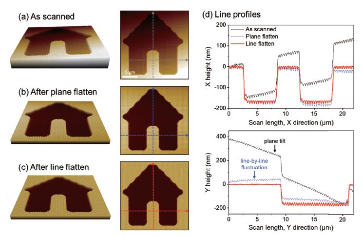
Fig. 2 Height images of a patterned wafer (a) as scanned, (b) after applying plane flattening to raw data, (c) after applying line-by-line flattening to raw data (3D view on the left and 2D view on the right), and (d) cross-sectional X and Y line profiles comparisons of the images in a (grey), b (blue), and c (red).
It can be inferred from Fig. 2(b) that inadequate or improper flattening parameters can distort the real data. This misinterpretation of data can lead to erroneous conclusions in the measurement result. For this reason, understanding the operation and data analysis of AFM is considerably important. EZ FlattenTM function has been developed to minimize time and effort needed in processing the AFM data. A machine learning-based algorithm is used to detect the surface features and apply an appropriate algorithm to flatten the data. Fig. 3 shows a screen capture of EZ Flatten function embedded in Park Systems’ SmartAnalysisTM data processing software. The only manual work required is loading the raw data and executing the function. Then, operators can select the best result among recommended output images. The function is expected to help enhance the productivity of measurements and minimize labor costs and human error in manual data processing.
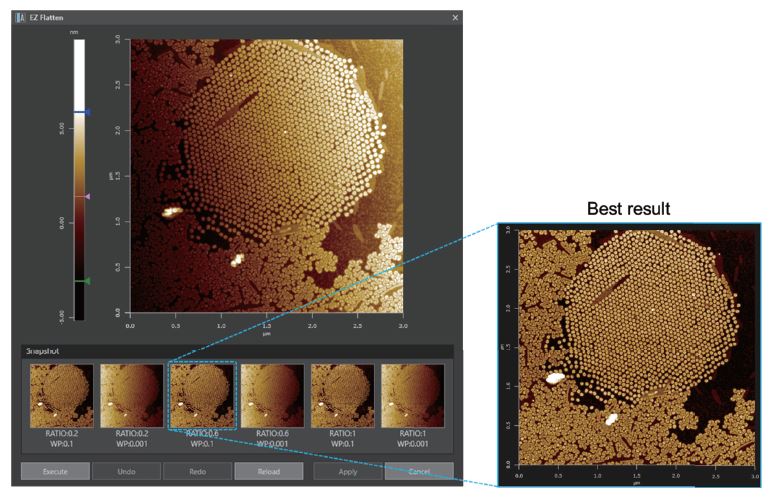
Fig. 3 Screen capture of EZ Flatten function. Up to six combinations of flattening parameters can be applied. Snapshots allow users to select the most appropriate result.
Selecting roughness parameter
Surface roughness is used as a parameter to quantify the surface properties of a material. Roughness represents quantitative height statistics and texture of a surface and is internationally used as a criterion to evaluate and compare the surface specifications. By monitoring and controlling the level of surface roughness, the target quality and performance of a surface can be adjusted. AFM allows quantification of surface roughness based on both profile (line roughness) and areal (surface roughness) methods.
Surface roughness parameters can be selected depending on the purpose of evaluation. For example, arithmetic average roughness (Ra), root mean square roughness (Rq), or peak-to-valley roughness (Rpv) are typically used parameters to evaluate the surface finishing quality in semiconductor manufacturing. Ra, Rq, and Rpv provide quantitative information on unevenness of the surface. However, in certain cases, the surface properties cannot be quantified solely based on these parameters. As shown in Figs. 4(a) and 4(b), two samples of the same peak-to-valley distance show identical Ra and Rq although their surface structures are vastly different. This outcome is due to the fact that Ra or Rq does not differentiate between peaks and valleys [13]. As a result, surfaces with different shapes can yield the same roughness value. Line profile (Fig. 4c) and height histograms (Fig. 4d) comparisons reveal a significant difference in height distribution between two samples due to structure difference. Surface changes of sample A are mainly composed of valleys, whereas sample B contains mostly peaks. In this case, skewness roughness (Rsk), which accounts for the deviation of the surface about the mean plane can be used to distinguish between two samples, as shown in areal roughness calculation result in Fig. 4(b). It can be seen from Fig. 4(d) that major height distribution of sample A skews above the mean line, resulting in a negative Rsk value. In contrast, height distribution skews beneath the mean line resulted in a positive Rsk value of sample B.
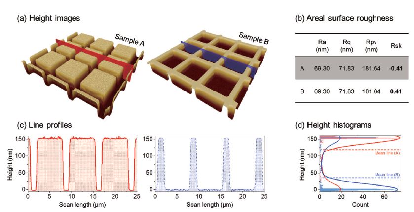
Fig. 4 (a) Height images, (b) areal surface roughness parameters, (c) line profiles, and (d) height histograms obtained on two patterned samples A and B. In (d), histograms and mean lines are determined from line profiles in (c).
Elevating surface measurement precision amid challenges
Beyond gaining a deep understanding of tip-sample interactions and refining data analysis skills, it is pivotal to proactively address challenges inherent in scanning probe techniques. This section delves into these nuances, providing insightful guidance to enhance measurement accuracy while also considering and mitigating the potential for inaccuracies in data analysis.
Tip-sample convolution
As a scanning probe-based technique, the AFM image is a map of the interaction between the AFM tip and sample. In other words, the AFM image is a convolution of the shape of the AFM tip and the shape of sample surface. Conventional AFM tips have a finite radius of curvature ranging from several nanometers to a few micrometers at the end, depending on specific applications. A general rule of thumb is to select a tip which radius is smaller than the surface features of the sample to be measured. A properly selected tip can reach even the deepest regions of the surface, allowing accurate reconstruction of sample surface. In contrast, a tip whose size is larger than the sample feature can make the surface features look wider and the valley looks shallower [14]. Tip-sample convolution also becomes more significant as the tip worn out during long-term measurement.
Fig. 5 presents an example of the effect of tip-sample convolution on measured surface properties. A patterned wafer was used as a sample. Firstly, an initial scan was performed in Non-contact mode to examine the true surface topography of the sample (‘Initial’ height image in Fig. 5a). Then, the same area was continuously scanned in Tapping mode for up to 35 repeats. The images at the 3rd, 6th, 7th, and 35th repeats are shown in Fig. 5(a). A relatively large tapping amplitude was used to intentionally induce wear to the AFM tip to study the effect of progressing tip wear on the measured surface properties. Finally, the scan mode is switched to Contact mode to introduce significant wear to the tip (‘After contact’ height image). As shown in height images and line profiles in Figs. 5(a) and 5(b), the surface step edge is getting blurry as the number of repeats increases, and a significant change can be observed after the final contact scan. Similarly, the wear progression of the tip can be confirmed from the line profiles at same location, as denoted by the dashed box in Fig. 5(b). The initial non-contact scan showed a clear shape of the surface step edges. As the number of repeated measurements increases, the tip is progressively worn out and the shape of the blunted tip is convoluted into the sample profile. As a result, the tip could not reach the bottom of the pattern and the tip side angle is reflected in the sidewall of the pattern.
The wear progression of the tip is also reflected in the roughness calculation result. Fig. 5(c) summarizes the Rq value calculated from line profiles in Fig. 5(b) with respect to the number of scans. The highest value of Rq was determined from the initial non-contact scan (black dot). It is assumed the initial sharp tip can reach the bottom of the pattern, resulting in the actual surface roughness of the sample. As the tip is worn out gradually during tapping scan, the Rq value gradually decreases as the number of scans increases until the 6th scan. A sharp decrease in Rq at the 7th scan suggests a major change in tip apex geometry, possibly due to fracture. The Rq value remains stable from the 7th to the 35th scan. A possible reason for this outcome is that the tip apex is flattened due to fracture, and a major increase in tip apex radius helps reduce tip wear [15]. The tip apex is significantly worn out due to contact scan, resulting in a sharp reduction of Rq at the final contact scan. The change of the tip apex was confirmed by performing AFM scan on a tip self-imaging grating, as shown in Fig. 5 (d). Profile comparison reveals a significant change in tip geometry due to wear before and after the entire set of measurements.
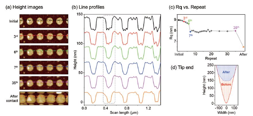
Fig. 5 (a) Height images, (b) cross-sectional line profiles comparison, (c) Rq values calculated from same line profiles with respect to the number of scans, and (d) tip end shape before and after measurement. For better observation, vertical shifts were applied to the line profiles in (b), and the color was matched between the height image, line profile, and Rq data.
A non-contact measurement using a different sharp tip showed no major change of the test area after measurement (results not shown), indicating that the change of tip shape is responsible for changes in height images, and therefore, roughness calculation results. The results suggest that preservation of the tip apex is crucial in obtaining an accurate surface measurement. The tip apex can be protected by using non-destructive imaging techniques such as Non-contact mode. In addition, tip wear can be minimized by selecting tips made of durable materials such as diamond. However, considering that a diamond tip typically has a larger curvature radius than a silicon tip, the tip should be selected in consideration of measurement targets. For example, for samples with well-separated steps (e.g., atomic steps of sapphire or SiC wafer), the tip sharpness does not significantly affect measurement result [16]. In such cases, a tip with a larger radius or a blunted tip may be more beneficial to preserve the tip geometry in consecutive measurement since wear progression of the tip generally reduces with increasing tip radius [15].
Monitoring the tip end
From the data in Fig. 5, it can be seen that changes in tip condition (e.g., increase in curvature radius due to wear) have a significant contribution to the surface measurement result. To better understand the effect of tip wear progression, it is recommended to monitor the tip condition during scanning, especially in long-term measurements. There are a few methods to monitor the tip apex such as tip imaging using scanning electron microscopy (SEM), self-imaging on a tip characterization grating, or monitoring changes in the shapes of amplitude- distance curve and force-distance curve. The basic principles, advantages, and limitations of each method are summarized in Table 2. For SEM imaging, the tip should be unmounted from the AFM system, which therefore, interrupts the workflow. For self-imaging, a tip characterization sample can be mounted to the same sample chuck of the AFM for convenience. However, the specific structure of characterization grating, as can be seen in Fig. (6a), may induce additional tip wear if scan parameters are not properly controlled. The force-distance monitoring method is based on an assumption that an increase in tip radius due to wear gives rise to an increase in tip-sample adhesion force [17,18]. This method is more appropriate for a tip-sample system that exhibits relatively strong adhesion properties. The amplitude-distance method relies on the dependency between tip sharpness and tip-sample atomic forces. Accordingly, a sharp tip exhibits a clear attractive-repulsive transitions in the amplitude-distance curve while a blunted tip shows a major contribution of attractive force [19,20].
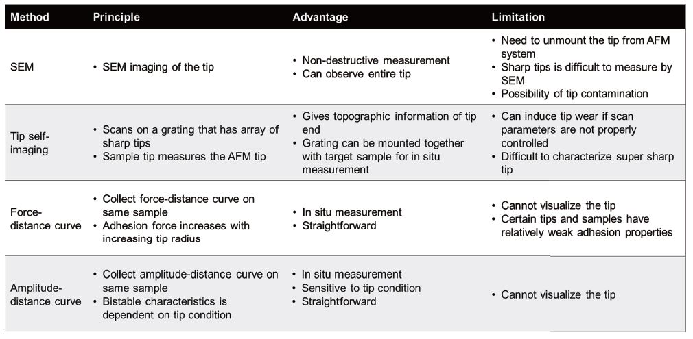
Table 2. Summary of methods to monitor the AFM tip end.
Fig. 6 presents an example of tip monitoring in AFM. The tip apex condition was monitored before and after measurement (result in Fig. 5) by using self-imaging, amplitude-distance curve, and force-distance curve methods. A clear difference in the tip shape was observed before and after measurement due to wear, as shown in Fig. 6(a). Tip wear can also be deduced based on changes in amplitude-distance and force-distance behaviors, as shown in Figs. 6(b) and 6(c). Among the methods, the amplitude-distance curve provides a reliable and straightforward characterization of tip end condition that can be performed in situ without the need of switching the sample or unmounting the tip from the AFM system.
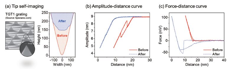
Fig. 6 AFM tip end monitoring using (a) tip self-imaging on a tip characterization grating (TGT1, TipsNano), (b) amplitude-distance curve, and (c) force-distance curve before and after measurement.
Measurement repeatability
To meet the requirements of a large-scale analysis tool, there are a few factors that should be considered when performing an AFM measurement, such as accuracy and repeatability of test, and tip-to-tip variation. Measurement accuracy is determined by how accurate the result is compared to actual values while repeatability is related to how the result is reproduced in multiple repetitions of measurements. Fig. 7 shows an example of a repeatability test on a calibration grating. A single tip was used to scan a calibration grating with a known step height in Non-contact mode of AFM. Three different tests were performed on three different days. Each test consisted of 100 repeats. The step height was determined to be 43.29 ± 0.10 (mean ± one standard deviation), 43.31 ± 0.08, and 43.28 ± 0.09 nm for test 1, test 2, and test 3, respectively. It was found that the mean step heights of the three tests agree well with each other. The relative error of each test is smaller than 0.2% and was possibly associated with sample changes due to temperature fluctuation during the long hours of measurement. The outcome suggests that the measurement is highly reproducible with minor variations. In addition, an agreement between the measured step height from the tests and expected step height provided by the manufacturer (43.3 ± 0.6 nm) can be observed from the data in Fig. 7(b), indicating high accuracy of the AFM measurements.
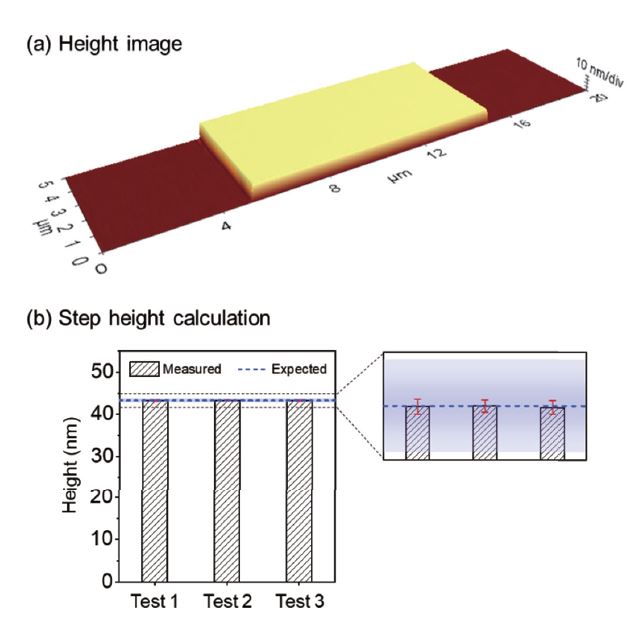
Fig. 7 (a) Height image obtained on a standard step height calibration grating (SHS8-440, VLSI), and (b) summary of step height measurement results from three tests. Error bars (red bars) of measured values represent one standard deviation of 100 repeats. Error band (blue gradient) of expected step height represents the error margin. Expected value and error band are independently measured by the manufacturer.
Fig. 8 presents an example of tip-to-tip variation tests. Four different tips of the same type were used to scan a Si wafer in Non-contact mode. A total number of 800 repeated scans was performed using each tip. Examples of height images obtained at the 1st and 800th scans using tips 1 and 2 are shown in Fig. 8(a). Ra values obtained from 4 tips are summarized in Fig. 8(b). A relative error of less than 1.9% calculated from 800 data collected using each tip confirms the measurement repeatability. Also, the deviation of Ra value from 4 measurements is determined to be 3.5%, possibly associated with a combination of tip-to-tip variation and position-to-position variation of the sample surface. A position-to-position variation of 5% is expected for this sample. Although it is difficult to distinguish the contribution of each factor, 3.5% total deviation suggests that the tip-to-tip variation is negligible. The result also proves the ability of Non-contact mode to preserve the tip and sample even after long hours of measurement.
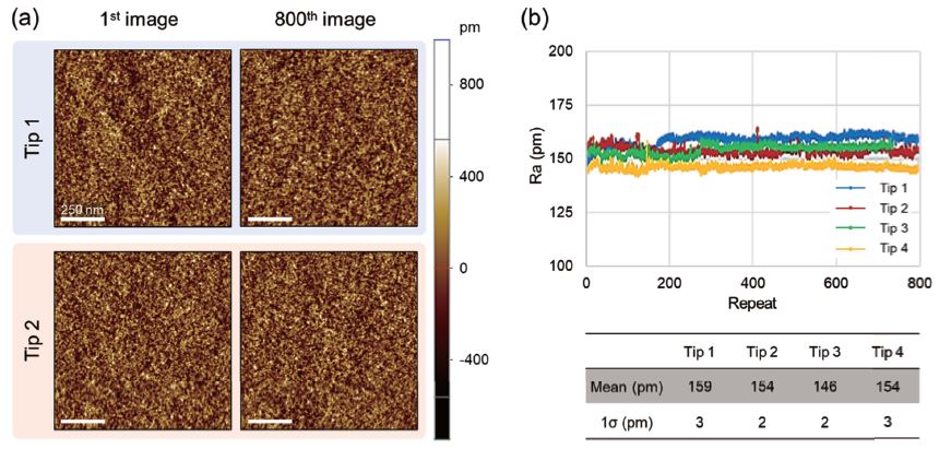
Fig. 8 (a) Examples of height image obtained at the 1st scan and 800th scan using tips 1 and 2, and (b) summary of Ra values determined from 800-image roughness measurement tests using 4 different tips of the same type.
Summary
This whitepaper overviews some aspects of surface properties measurement at the nano-scale using the AFM. It was expected that the outcome would add useful information for an accurate measurement of surface properties based on understanding of interactions between the AFM tip and sample. There are a few checkpoints that need to be considered when measuring a surface:
• In general, Non-contact mode is a good choice to obtain surface topography with minimized artifacts while preserving tip and sample. • The scan size can be selected by considering the wavelengths of waviness and roughness, depending on the target application. • Flattening in first order is often used to level the surface slope. Beware that higher orders of flattening may alter the actual data. • Roughness parameters can be selected in consideration of surface characteristics. While Rq and Ra are typically used, it is recommended to find a proper roughness parameter for your specific case. • Tip-sample convolution is a non-trivial issue of AFM. Understanding tip-sample interactions helps a proper interpretation of the AFM result.
References
[1] D. Zhao, X. Lu, Chemical mechanical polishing: Theory and experiment, Friction. 1 (2013) 306–326.
[2] W. Xie, Z. Zhang, L. Liao, J. Liu, H. Su, S. Wang, D. Guo, Green chemical mechanical polishing of sapphire wafers using a novel slurry, Nanoscale. 12 (2020) 22518–22526.
[3] C. Gui, M. Elwenspoek, N. Tas, J.G.E. Gardeniers, The effect of surface roughness on direct wafer bonding, J. Appl. Phys. 85 (1999) 7448–7454.
[4] M.R.S. Soares, C.A.R. Costa, E.M. Lanzoni, J. Bettini, C.A.O. Ramirez, F.L. Souza, E. Longo, E.R. Leite, Unraveling the Role of Sn Segregation in the Electronic Transport of Polycrystalline Hematite: Raising the Electronic Conductivity by Lowering the Grain-Boundary Blocking Effect, Adv. Electron. Mater. 5 (2019) 1900065.
[5] F.C. Salomão, E.M. Lanzoni, C.A. Costa, C. Deneke, E.B. Barros, Determination of High-Frequency Dielectric Constant and Surface Potential of Graphene Oxide and Influence of Humidity by Kelvin Probe Force Microscopy, Langmuir. 31 (2015) 11339–11343.
[6] H. Song, Y. Ma, D. Ko, S. Jo, D.C. Hyun, C.S. Kim, H.-J. Oh, J. Kim, Influence of humidity for preparing sol-gel ZnO layer: Characterization and optimization for optoelectronic device applications, Appl. Surf. Sci. 512 (2020) 145660.
[7] R.Y.K. Yoo, Automated AFM Boosts Throughput in Automatic Defect Review, Micros. Today. 22 (2014) 18–23.
[8] F. Nagano, S. Iacovo, A. Phommahaxay, F. Inoue, F. Chancerel, H. Naser, G. Beyer, E. Beyne, S. De. Gendt, Void Formation Mechanism Related to Particles During Wafer-to-Wafer Direct Bonding, ECS J. Solid State Sci. Technol. 11 (2022) 63012.
[9] S. Wang, Q. Liu, C. Zhao, F. Lv, X. Qin, H. Du, F. Kang, B. Li, Advances in Understanding Materials for Rechargeable Lithium Batteries by Atomic Force Microscopy, Energy Environ. Mater. 1 (2018) 28–40.
[10] G. Binnig, C.F. Quate, C. Gerber, Atomic Force Microscope, Phys. Rev. Lett. 56 (1986) 930–933.
[11] Y. Martin, C.C. Williams, H.K. Wickramasinghe, Atomic force microscope–force mapping and profiling on a sub 100‐Å scale, J. Appl. Phys. 61 (1987) 4723–4729.
[12] Q. Zhong, D. Inniss, K. Kjoller, V.B. Elings, Fractured polymer/silica fiber surface studied by tapping mode atomic force microscopy, Surf. Sci. Lett. 290 (1993) L688–L692.
[13] B. Bhushan, Surface roughness analysis and measurement techniques, in: Mod. Tribol. Handbook, Two Vol. Set, CRC press, 2000: pp. 79–150.
[14] P. Eaton, K. Batziou, Artifacts and Practical Issues in Atomic Force Microscopy BT - Atomic Force Microscopy: Methods and Protocols, in: N.C. Santos, F.A. Carvalho (Eds.), Springer New York, New York, NY, 2019: pp. 3–28.
[15] K.-H. Chung, Y.-H. Lee, H.-J. Kim, D.-E. Kim, Fundamental Investigation of the Wear Progression of Silicon Atomic Force Microscope Probes, Tribol. Lett. 52 (2013) 315–325.
[16] F. Gołek, P. Mazur, Z. Ryszka, S. Zuber, AFM image artifacts, Appl. Surf. Sci. 304 (2014) 11–19.
[17] B. Gotsmann, M.A. Lantz, Atomistic Wear in a Single Asperity Sliding Contact, Phys. Rev. Lett. 101 (2008) 125501.
[18] J. Liu, Y. Jiang, D.S. Grierson, K. Sridharan, Y. Shao, T.D.B. Jacobs, M.L. Falk, R.W. Carpick, K.T. Turner, Tribochemical Wear of Diamond-Like Carbon-Coated Atomic Force Microscope Tips, ACS Appl. Mater. Interfaces. 9 (2017) 35341–35348.
[19] S. Santos, L. Guang, T. Souier, K. Gadelrab, M. Chiesa, N.H. Thomson, A method to provide rapid in situ determination of tip radius in dynamic atomic force microscopy, Rev. Sci. Instrum. 83 (2012) 43707.
[20] A. Temiryazev, S.I. Bozhko, A.E. Robinson, M. Temiryazeva, Fabrication of sharp atomic force microscope probes using in situ local electric field induced deposition under ambient conditions, Rev. Sci. Instrum. 87 (2016) 113703.