
Teflon Defect on SiO₂
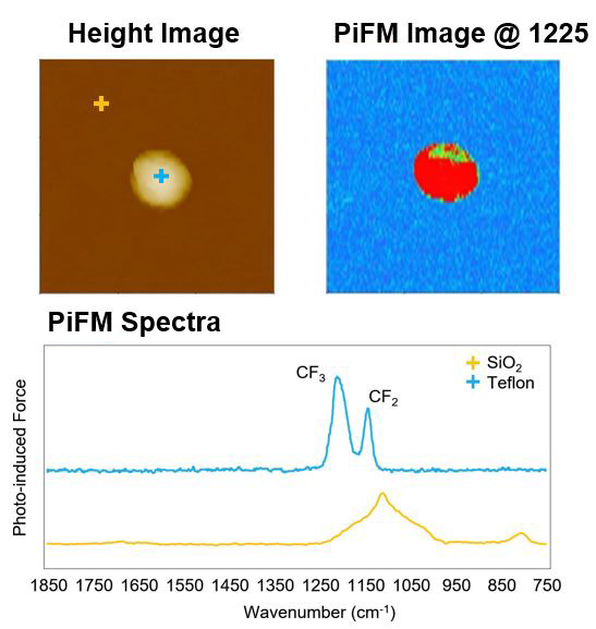
This slide shows the analysis of a Teflon defect on a SiO₂ substrate.
The AFM topography image reveals the defect location and structure on the surface.
The PiFM chemical image then highlights the contrast between the Teflon region and the surrounding SiO₂.
The IR spectra confirm the chemical identity by showing characteristic absorption peaks of Teflon that are absent in the SiO₂ background.
Together, these results demonstrate how PiFM correlates morphology with chemical specificity at the nanoscale.
Scanning Conditions
- System: Nano-IR
- Scan Mode: PiFM (Channel: Z Height, PiFM Amplitude)
- Scan Rate: 0.1 Hz
- Scan Size: 300 µm × 300 µm
- Pixel Size: 512 × 64 pixels
Related Contents


×