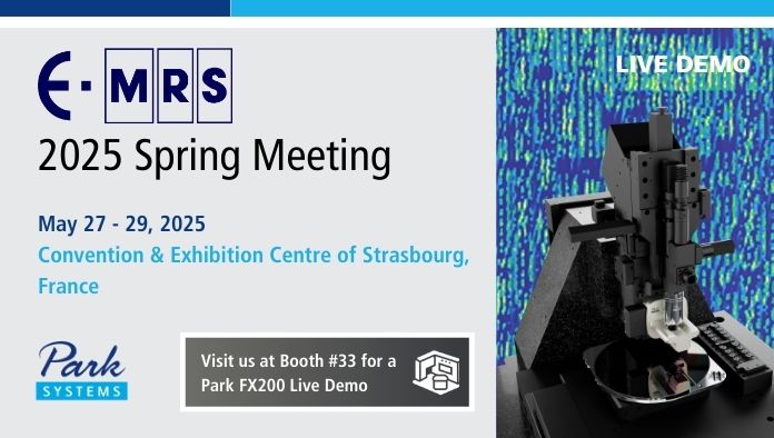
The 2025 Spring Meeting of the European Materials Research Society (E-MRS) will take place at the Convention & Exhibition Centre of Strasbourg from May 26 to 30, 2025. The conference will feature 23 parallel symposia, a plenary session, and an exhibition showcasing products and services relevant to materials science. Around 80 international exhibitors will present a wide range of equipment, products, and services, providing attendees with opportunities for hands-on demonstrations and face-to-face interactions with company representatives. Park Systems will be amongst the exhibitors, showcasing our new FX200 AFM live at our booth.
- Exhibition Date: 27-29 May 2025
- Location: Convention Centre of Strasbourg, France
- Booth: #33
- Link: https://www.european-mrs.com/meetings/2025-spring-meeting
Join our talk on Tuesday, May 27th at 2:45 pm in Symposium E07 “Novel Materials and Processes for Neuromorphic Applications”
Title: “A tale of struggle or How to optimize electric characterization on the nm scale”
Presenter: Dr. Alexander Klasen, Principal Scientist, Park Systems Europe
Co-Author: Dr. Andrea Cerreta, Principal Scientist, Park Systems Europe
Abstract:
Memristors are a novel class of electronic elements, that change their electric resistance depending on the history of current that was transported through that element.[i] First reported in 2007 by D. B. Strukov, doped TiO2 thin films have been intensively studied as they represent the first practical example of a memristor.[ii] However, to better understand such systems, we need to investigate correlated local properties such as morphology, local conductance, or work function.
Here, atomic force microscopy is a well-established tool for characterizing surfaces and interfaces with nm-resolution. The utilization of a nanometric probe in close proximity to the sample allows for a series of advanced characterizations of the material ranging from topography to local current flow, surface potentials, or even mechanical features like adhesion and stiffness. However, such measurements can be challenging and time-consuming as a multitude of effects with sometimes opposing influences on local conductance can take place.
This talk provides a tale of struggle of how to obtain local current measurements on different TiO2 thin films on modified FTO substrates using conductive atomic force microscopy.[iii] We discuss how different surface treatments affect the surface/interface defect density of metal oxides and the respective effect on the local measured current. Lastly, we present Park Systems' state-of-the-art FX40 atomic force microscope that allows for advanced scripting, fully automated tip exchange, and tip-sample approach while enabling seamless switching from CAFM to Kelvin Probe Force Microscopy or mechanical characterization without the need to change either the cantilever or AFM hardware.
[i] Leon O. Chua Memristor. IEEE Trans, Circuit Theory, 1971, CT-18 (5), 507-519.
[ii] Strukov, D.B.; Snider, G.S; Stewart, D.R.; Williams, R.S. The Missing Memristor Found Nature 2008, 453 (7191), 80-83.
[iii] Klasen, Alexander, Synthesis and Analysis of Thin Films for Perovskite Solar Cells, Johannes Gutenberg-Universität Mainz

