
The Multifrequency AFM conference series is a platform for experts and newcomers in force microscopy and nanomechanics to share knowledge on advanced force microscopy. Key topics of the 10th edition include machine learning methods for AFM, nanomechanics, high-speed AFM, and high-resolution imaging of soft matter and solid-liquid interfaces.
Park Systems is proud to be a part of this event as a sponsor, exhibitor and with a talk. Visit our booth for a live demonstration of the Park FX40 AFM.
- Date: 26-30 May 2025
- Location: Institute of Materials Science of Madrid (ICMM-CSIC), Spain
- Link: https://wp.icmm.csic.es/multifrequency-afm/
Join our talk – date and time to be confirmed.
Title: “Characterizing the electronic properties of graphene on silicon carbide via Atomic Force Microscopy”
Presenter: Dr. Andrea Cerreta ,Principal Scientist, Park Systems Europe
Co-Author: Dr. Alexander Klasen, Principal Scientist, Park Systems Europe
Abstract:
The rising interest towards two-dimensional (2D) layered materials is motivated by their exotic behaviour and possible nanotechnological applications [1,2]. Such systems are formed by a single atomic layer such as graphene, boron nitride, transition metal dichalcogenides or by their stacking. The interplay of chemical and geometrical factors (the type of stacked layers, the out-of-plane relative alignment of their unit cells, the twisting angle, and the presence of strain or defects) leads to new material properties.
Stacking methods rely on the manual exfoliation and subsequent deposition of single layers at peculiar angles to obtain the desired behaviour. It has been reported the possibility of rotating the top layer of heterostructures by means of AFM [3], but the tuning of the geometry of such multilayers remains challenging. Silicon carbide (SiC) is a known precursor of graphene used to produce large-sized flakes of graphene via thermal decomposition. As a result of such a treatment, Si atoms leave the top layers of the crystal, leading to the formation of epitaxial single- or multi-layered graphene, whose electronical properties have been characterized also by AFM [4]. This reproducible way of obtaining graphene stacks on the top of a tunable wide-band-gap semiconductor makes it an interesting system to further characterize at nanoscale.
Here, we show several examples of AFM-based analysis of these structures. In particular, a mapping of the layer-dependent surface potential via heterodyne Kelvin Probe Force Microscopy (KPFM) on differently prepared SiC samples will be presented. Conductive AFM (C-AFM) experiments performed on the same areas show triangular and stripe-like domains to correlate to the number of stacked layers and to the KPFM signal. Finally, we demonstrate how electronic information about individual graphene flakes on insulating SiC can be obtained using scanning Microwave Impedance Microscopy (sMIM) to overcome the impossibility to apply a bias to graphene.
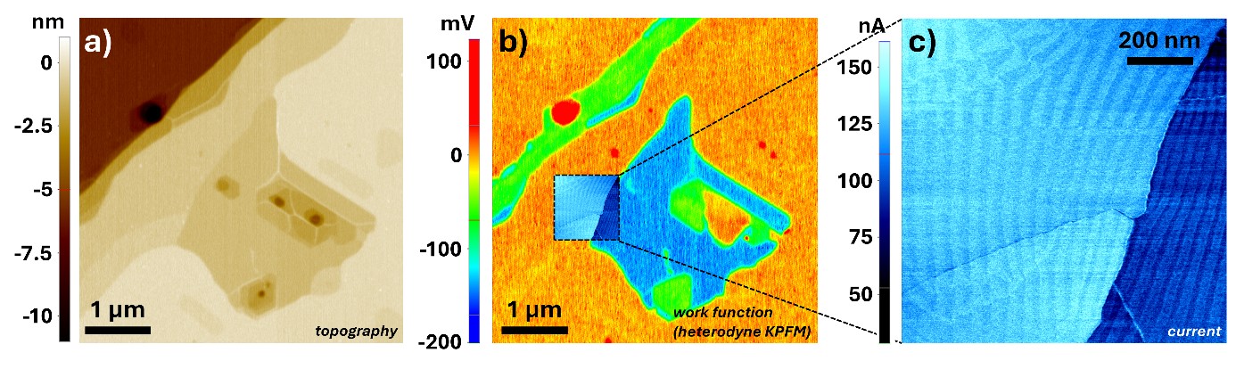
Fig. 1: a) topography and b) work function maps on the same area of a SiC sample; c) current map at constant voltage on an area of previous images. The sample was provided by Dr. Rejhon from Institute of Physics, Charles University, Prague, Czech Republic.
[1] X. Wang et al., Nat. Nanotechnol. 17, 367–371 (2022)
[2] C. R. Woods et al., Nat. Commun. 12, 347 (2021)
[3] R. Ribeiro-Palau et al., Science 361, 690-693 (2018)
[4] M. Rejhon et al., PNAS 121, e2408496121 (2024)