QuickStep SCM Mode
High Throughput QuickStep Scan
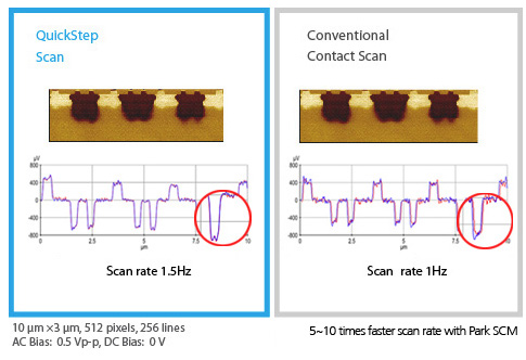
With the implementation of QuickStep scan, the throughput of the SCM measurement was dramatically increased, as much as ten times the standard SCM scan speeds, without compromising signal sensitivity, spatial resolution or data accuracy. In QuickStep scan, the XY scanner stops at each pixel point to record the data. It makes a fast jump between the pixel points.
- Ten times faster than conventional SCM scan
- No compromise of signal sensitivity, spatial resolution, or data accuracy
QuickStep Scan
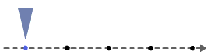
Rather than continuous movements, the XY scanner stop at each data acquisition point.
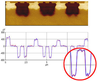
Scan rate 1.5Hz
Conventional Scan

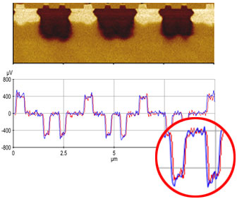
Scan rate 1Hz
Scan size: 10µm×3µm, AC Bias: 0.5 Vp-v, DC Bias: 0 V
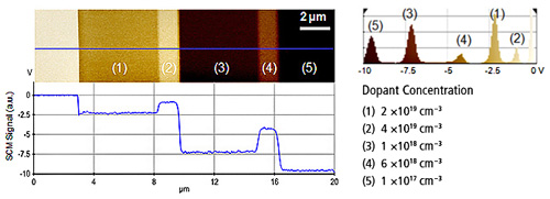
Accurate Dopant Profiling by Park SCM
In semiconductor manufacturing, the ability to characterize the dopant profile is important in identifying causes of failure as well as in making design advancements. For device characterization, scanning capacitance microscopy (SCM) provides the unique ability to measure quantitative 2D dopant profiles.
PinPoint Conductive AFM Mode
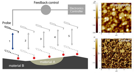
PinPoint Conductive AFM was developed for well defined electric contact between the tip and the sample. They XY scanner stops during the electric current acquisition with contact time controlled by a user. PinPoint Conductive AFM allows higher spatial resolution, without lateral force, with optimized current measurement over different sample surface.
PinPoint Mode
Contact
Tapping
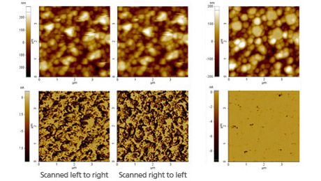
Sample: ZnO nano-rods, -3 V sample bias
The comparison of conductive AFM images of ZnO nanorods show that the conventional contact conductive AFM may have a higher current measurement than tapping conductive AFM, but its resolution is compromised as the tip wears out in contact mode topography. The new PinPoint conductive AFM shows the best of both higher spatial resolution and optimized current measurement.
High-bandwidth, Low-noise Conductive AFM
Conductive AFM is an important tool in various device research, especially failure analysis in industry. Park conductive AFM has the most competitive specification in the market, having both the lowest current noise level in the industry and the largest gain range.
- The lowest current noise level in the industry (0.1 pA)
- Maximum current in the industry (10 μA)
- Largest gain selection covers 7 orders of magnitude (103 ~109)
Park NX20 advanced SPM modes (*Optionally available)
Standard Imaging
- True Non-Contact™ Mode
- PinPoint™ AFM
- Basic Contact AFM
- Lateral Force Microscopy (LFM)
- Phase Imaging
- Intermittent (tapping) AFM
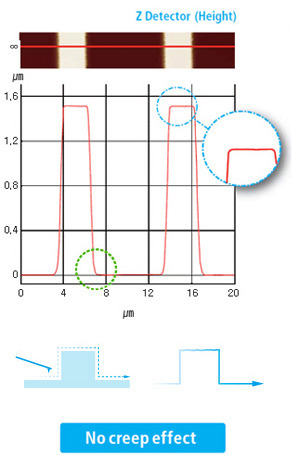
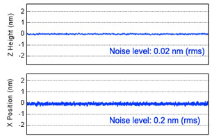
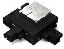
 The XY
scanner consists of symmetrical 2-dimensional flexure and high-force piezoelectric stacks provides high
orthogonal movement with minimal out-of-plane motion as well as high responsiveness essential for precise sample
scanning in the nanometer scale.
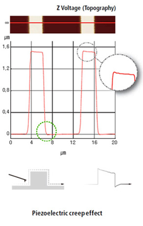
The XY
scanner consists of symmetrical 2-dimensional flexure and high-force piezoelectric stacks provides high
orthogonal movement with minimal out-of-plane motion as well as high responsiveness essential for precise sample
scanning in the nanometer scale.