


To aid in the development of advanced semiconductor devices, techniques such as Spreading resistance profiling (SRP), Secondary ion mass spectrometry (SIMS), and Scanning capacitance microscopy (SCM) and many others have been developed. Currently Scanning spreading resistance microscopy (SSRM) is attracting attention as a promising technique for studying the electrical characteristics of semiconductor devices. SSRM is a technique based on scanning probe microscopy (SPM), in which a conductive material-coated tip scans a biased sample surface and measures electrical properties such as current, conductance, and resistance of the samples. Using a logarithmic amplifier, it can simultaneously measure a wide range of conductive materials from insulators and semiconductors to metals. In ambient conditions, metal or semiconductor surfaces can be covered with an insulating oxide layer. However, ohmic contact between the tip and sample is essential to accurately investigate the resistance of a sample. Here, SSRM is a highly efficient technique for 2D carrier profiling of semiconductors since it allows directly contacting the sample surface by stripping the oxide layer while imaging with a durable diamond AFM tip. SSRM usually requires a high tip-sample contact force to cut through the oxidation or contamination layer on the sample surface. Moreover, it is recommended to measure the sample in a vacuum state or nitrogen atmosphere to prevent re-oxidation or water adsorption on the sample surface while measuring.
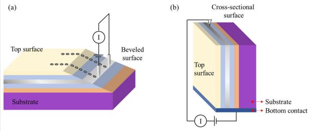
Figure 1. Schematic diagrams of (a) SRP and (b) SSRM
In addition, a logarithmic current amplifier is required to measure a wide range of resistance as a linear current amplifier can only measure a narrow range of current that depends on the amplifier gain. Yet, semiconductor device structures generally consist of metal, semiconductor and oxide layers, and those different materials have a resistance range varying from ohm to giga ohm. SSRM is an implementation of a wellestablished SRP method used on a microand nano-scale for cross-sectioned sample surfaces. A generic SRP, however, is a dual probe technique that uses large probes of approximately 1 μm in radius, while SSRM uses an AFM tip with only a few tens of nm in radius, which scans a small device region. Figure 1 shows the schematic diagram of SRP and SSRM. In SRP, the resistance is measured between two large probes on a beveled surface whereas in SSRM, the resistance is measured between a back-contact and the AFM tip on a cross-sectional surface to avoid the beveling related carrier-spilling effects. In SSRM, the resistance is calculated from Ohm’s law (R = V/I) and the spatial resolution depends on the radius of curvature at the apex of the AFM tip. The accuracy of resistance depends on how much the contact resistance can be reduced between tip and sample by increasing the contact force on the tip. To form an excellent Ohmic contact between tip and sample, a clean sample surface, environmental control, and a high contact force are recommended. In this regard, an AFM probe with a stiff lever and a rigid tip is preferred.
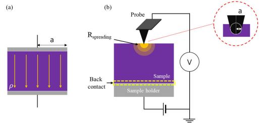
Figure 2. Schematic images of (a) general current flow between parallel metal plates and (b) spreading current flow between AFM tip and sample back-contact.
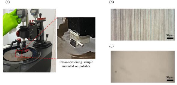
Figure 3. (a) Example of a polisher and cross-sectioning sample. Optical camera view on (b) an insufficient polished surface and (c) a well-polished surface.
As shown in figure 2 (a), in general, current flows through the whole area of the sample. However, when contacting the sample with a sharp AFM tip, the local current spread near the tip can be measured by SSRM due to the narrow contact area between the tip and the sample (figure 2 (b)). For an ideal case, the spreading resistance is RS = ρ/4a, where ρ is the local sample resistivity and a is the contact area represented by tip radius. Here, rough samples can change the effective contact area between the AFM tip and the surface, making accurate resistance value measurements difficult. Accordingly, polishing and subsequent cleaning can help to observe accurate doping profiles of a sample. Figure 3 (a) shows a polisher used to reduce the roughness of a cross-sectional sample and figure 3 (b) and (c) show examples of optical images of sample surfaces after (b) insuficient and (c) sufficient polishing.
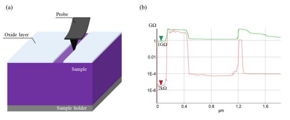
Figure 4. a) Schematic image of an SSRM measurement. The tip scans the sample removing the insulating surface oxide layer. (b) line profile comparison of the measured resistance on an oxide layer with high loading force (red) and low loading force (green).
As mentioned above, the ohmic contact between the tip and sample is also critical. An oxide layer will increase the contact resistance, creating a Schottky-barrier that will prevent the user from obtaining the correct resistance value. Figure 4 demonstrates how the tip scans the sample while removing the oxide layer and thus effectively minimizing the contact resistance (figure 4 (a)). The line profile in figure 4(b) exemplifies how the surface resistance changes by varying the loading force on the tip. In figure 5, an IFX dopant calibration sample (SSRM reference sample “NP20” made by Infineon) was investigated using SSRM with a 1.5 VDC sample bias. The sample has 20 different dopant states with phosphorusimplanted n-type areas and boron-implanted p-type areas on a Si substrate. The SSRM resistance image (figure 5 (a)) and line profile (figure 5 (b), next page) indicate the different resistances in each of the 20 dopants states using a logarithmic current amplifier to cover the full dynamic range of resistance.
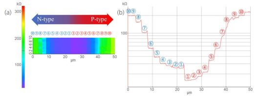
Figure 5. (a) SSRM resistance image. (b) line profile of IFX dopant calibration sample (NP20) which consists of 20 different n-type and p-type implant areas with a 1.5VDC sample bias
Figure 6. (c) dopant type and concentration of the sample.
Figure 6 (next page) shows SSRM images on the cathode surface of a rechargeable lithium-ion battery, which is typically used in a wide range of applications such as laptops, mobile phones, tablet computers, and automobiles. Lithium-ion battery samples should be handled under highly controlled environmental conditions because they are very sensitive to exposure to humidity and even nitrogen. To prevent damage to the lithiumion battery, the sample was measured under vacuum conditions in the NX-Hivac system. The electrical resistance distribution of highly conductive materials, polymer binders, and active materials is clearly observed as shown in figures 6 (b) and (d).