


-
Scratch Change CP-AFM Pattern FAPbI3 fifber TungstenDeposition MechanicalProperty PpLdpe PatternedSapphireSubstrat MESA structure BTO HydroGel Magnetostrictive YszSubstrate Lateral IcelandSpar Boron Composition Bio C60H122 Cobalt LaAlO3 SiWafer SKKU ScanningSpreadingResistanceMicroscopy Hydroxyapatite Polymer SingleCrystal HardDisk Piezo NUSNNI Ananth CancerCell CNT
Report image
If you found this image unacceptable, please let us know. We will review your report and take action if we determine this image is really unacceptable.
Atomic steps on GaP(Gallium Phosphide) layer on Si
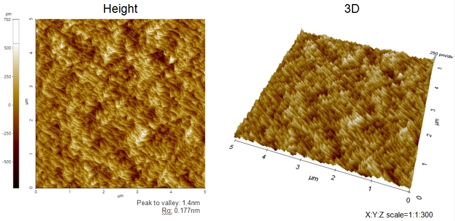
Scanning Conditions
- System: NX20
- Scan Mode: Non-contact
- Cantilever: PPP-NCHR (k=42N/m, f=300kHz)
- Scan Size: 5μm×5μm
- Scan Rate: 1Hz
- Pixel: 512×512