


-
lift_mode GalliumPhosphide PvdfBead HumanHair Alloy FAPbI3 Worcester_Polytechnic_Institute Implant NtuEee Hexylthiophene P3HT tip_bias_mode SicMosfet DomainSwitching StyreneBeads DNAProtein HOPG PS_PVAC ContactModeDot Display F14H20 Gold CarbonNanotube HiVacuum Perovskite UTEM doped Etch mechanical_property HexacontaneFilm TungstenDeposition HanyangUniv NTU PolycrystallineFerroelectricBCZT Cell
Report image
If you found this image unacceptable, please let us know. We will review your report and take action if we determine this image is really unacceptable.
Atomic steps on GaP(Gallium Phosphide) layer on Si
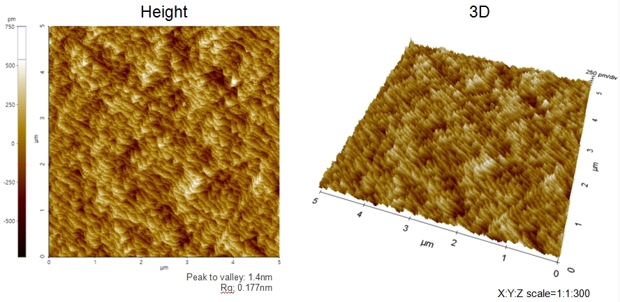
Scanning Conditions
- System: NX20
- Scan Mode: Non-contact
- Cantilever: PPP-NCHR (k=42N/m, f=300kHz)
- Scan Size: 5μm×5μm
- Scan Rate: 1Hz
- Pixel: 512×512