


Analysis of Thin-Film Coatings on Curved Surfaces by Spectroscopic Imaging Ellipsometry
Matthias Duwe
Table of Contents
Introduction
Imaging ellipsometry: concepts and setup
Imaging ellipsometry: concepts and setup
- Layer-thickness of ITO coating
- Layer-thickness of SiO2 top-layer antireflection coating
Summary
Imprint
Introduction
This slide-show shall provide a brief introduction for our proof-of-concept studies regarding the application of Spectroscopic Imaging Ellipsometry (SIE) for the analysis of thin-film coatings on curved surfaces. The primary scope of this study is to demonstrate measurements of layer-thickness distributions across microscopic lenses, i.e. the quantitative characterization of the metrology of the respective anti-reflection coatings. As a case study, we will present layer-thickness measurements of one-layer and two-layer coatings on two different microlens arrays.
We chose micro optics for this case study as our company’s flagship product, the imaging ellipsometer ep4, copes with this task without any need for special hardware adaptions. The general concepts developed, however, may also be applied to larger-scale, curved optics or other free-form objects. In those cases, application-specific hardware adaptions (e.g. sample positioning) might be required.
Abstract of Results
Using Spectroscopic Imaging Ellipsometry (SIE), we managed to measure the thickness distributions of thin-film coatings on two microlens arrays (MLA) with sub-nanometer thickness resolution and x-y-resolution of 4 µm or better
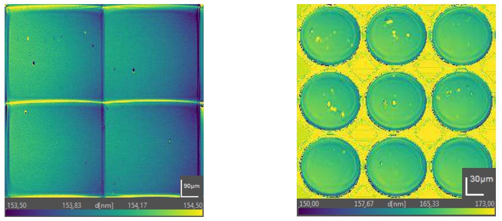
Measured thickness distribution of custom-made Indium-Tin Oxide (ITO) coating on square-grid MLA. / Measured thicknesses of top-layer antireflection coating (SiO2) on commercially available MLA
Imaging ellipsometry: concepts and setup
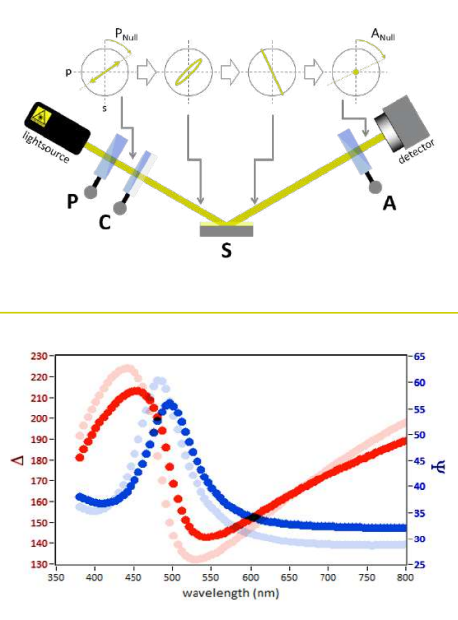
Ellipsometry
- Ellipsometry analyzes the change of polarization of light reflected from a sample
- yields information about film properties like thickness, refractive index and absorption
- optical components polarizer (P), compensator (C) and analyzer (A) are used
- change on polarization is described by the ellipsometric angles Delta(△) and Psi (ψ)
- △ and ψ are measured against wavelength (λ) and/or angle of incidence (AOI)
- film properties are obtained by fitting a numerical model to measurement data
Imaging Ellipsometry
Ellipsometry + Microscopy => lateral ellipsometric resolution down to 1 µm
- ψ(Psi), △(Delta) describe the change in the state of polarization induced by investigated sample
- ψ and △ are recorded for the each pixel of the field of view
- fitting of ψ and △ to a numerical model yields maps of:
- thickness (left)
- optical-constants (n, k) (right) volume-fraction etc.
- volume-fraction etc.
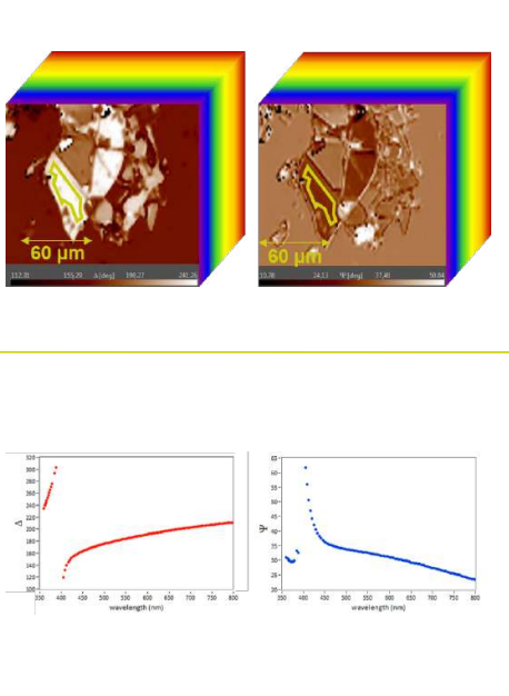
Micromapping of △ and ψ
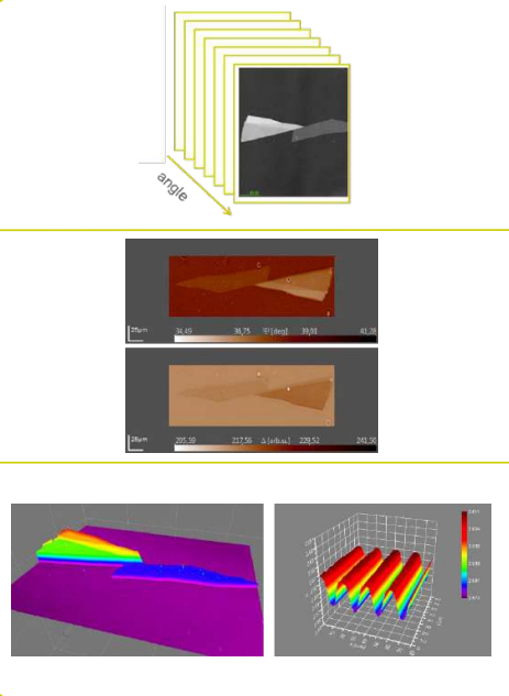
- △ and ψ maps are recorded for different wavelengths to obtain spectroscopic maps
- with the pixelshot tool, any region can be selected after the measurement to extract the corresponding spectra of △ and ψ
- these spectra of△ and ψ can be used to fit for layer thickness, optical parameters, etc.
- accordingly, spectra extracted on a pixel-by-pixel basis convert into maps of layer thickness, optical properties, etc.
Pixelshot on Spectroscopic Maps
- △ and ψ maps are recorded for different wavelengths to obtain spectroscopic maps
- with the pixelshot tool, any region can be selected after the measurement to extract the corresponding spectra of △ and ψ
- these spectra of △ and ψ can be used to fit for layer thickness, optical parameters, etc!
- accordingly, spectra extracted on a pixel-by-pixel basis convert into maps of layer thickness, optical properties, etc.
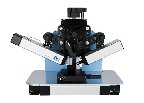
EP4 Spectroscopic Imaging Ellipsometer
Spectroscopic configuration*
• Xenon lamp + monochromator (360-1000 nm)
• LED hub (6 wavelengths)
Objective lenses*
• NA 0.13
• NA 0.21
• NA 0.35
Imaging ellipsometry: concepts and setup
Layer-thickness of ITO coating
Microlens Array 1: ITO-Coating Analysis
Here, we present a study of a custom-made*, single-layer coating of ITO (nominal thickness 150 nm) deposited on commercially available MLA of spherical lenses (radius of curvature 6.5 mm, square grid with 500 µm pitch, without apertures, substrate: fused silica).
For thickness analysis, we acquired hyperspectral images of A & 4 within the spectral range of 385 to 940 nm (in steps of 15 m) using a field of view of 1×1 mm² at an x-y-resolution of 4 um.
For data analysis, we first selected the (approximate) lens apex region (see highlighted regions) from the stack of hyperspectral ǻ & Ȍ images, and extracted the corresponding ellipsometric spectra. We used a numerical model of the sample to fit for ITO layer thickness along with the AOI-offset which accounts for unknown misalignment of the evaluated sample spot.
Results:
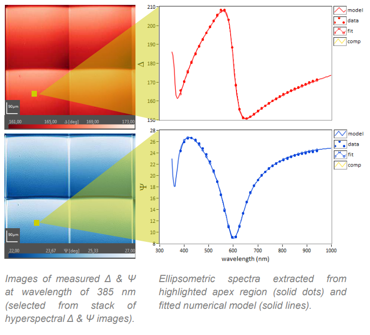
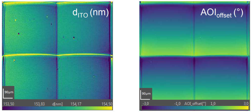
Secondly, we used the established numerical model to perform this fit procedure on a pixel-by-pixel basis Thus, we converted our stack of hyperspectral A & W images into maps of ITO layer thickness (left) and AOl-offset* distribution (right). The obtained layer thickness distribution features a gradient for each microlens that is oriented along the image's horizontal axis (left figure). This gradient is on the order of just 1 nm in total across each lens. This confirms our technique's capability of performing thin-film measurements on a curved surface with sub-nanometer thickness resolution.
Layer-thickness of SiO2 top-layer antireflection coating
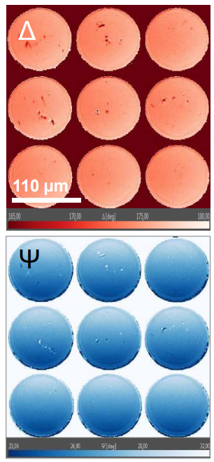
Microlens Array 2: SiO2-Coating Analysis
As a second sample application, we present a study on a two-layer antireflection coating of a commercially available MLA that has a significantly smaller radius of curvature (0.7 mm) than the one presented in the first example. That is why this sample required a MuellerMatrix based measurement combined with a proprietary analysis for curved-surface metrology that was developed by Accurion*
The inter-grid spacing between the circular microlenses feature Chromium apertures, and the lenses are made of fused silica. The MLA’s antireflection coating is a two-layer design, with the top layer made of SiO2. The thickness distribution of this top layer is the subject of this case study.
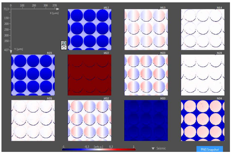
Imaging Mueller-Matrix Ellipsometry (IMME) is an advanced measurement mode that is available as an upgrade package for the imaging ellipsometer ep4. This mode measures 11 images of the smaple's Mueller matrix* whereas the standard mode would only yield the two images of △ & ψ. This additional data provides the essential information which is needed to measure thin-film coatings on *The Mueller matrix is the most general description of the VDPSOHµV interaction with polarized light. coatings on strongly curved surfaces.
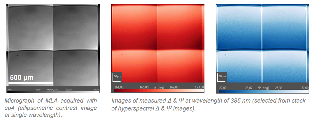
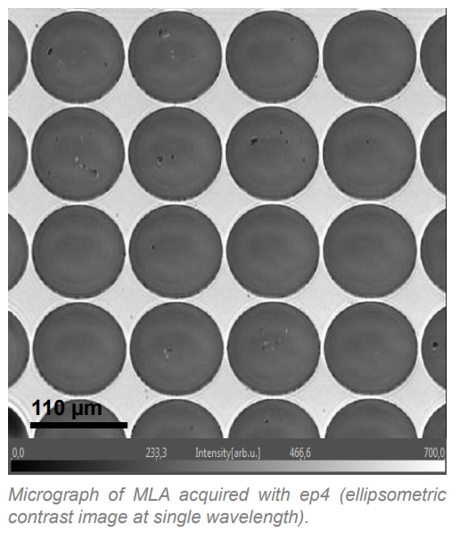
IMME images at a single wavelength (selected from stack of hyperspectral IMME images).
For data analysis, we use Accurion's proprietary algorithm to extract isotropic sample parameters* △ & ψ from the measured Mueller matrix (PATENT PENDING). This algorithm works without any prior knowledge of the surface geometry. Its only input is the measured Mueller matrix micrograph.
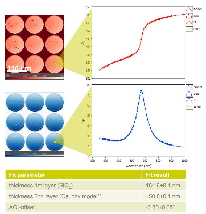
MM micrograph (left) and ǻ & Ȍ maps extracted thereof (top right and bottom right images, respectively).
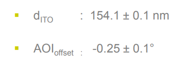
For the measurement of the SiO2 top-layer thickness, we acquired hyperspectral images of the Mueller matrix within the spectral range of 380 to 1000 nm (in steps of 20 nm) using a field of view of approximately 0.5x0.5 mm2 at an x-y-resolution better than 4 µm. The set of hyperspectral Mueller matrix micrographs then translated into a set of hyperspectral ǻ & Ȍ micrographs. From hereon, the analysis procedure is essentially the same as for the first application:
1. Establishing a model at the lens apex.
2. Calculating SiO2 layer thickness pixel-by-pixel from hyperspectral stack of ǻ & Ȍ micrographs
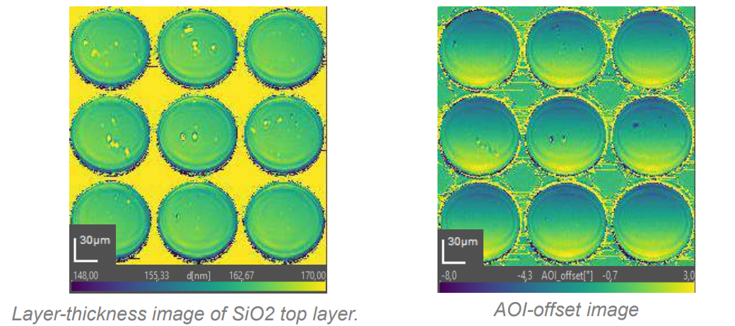
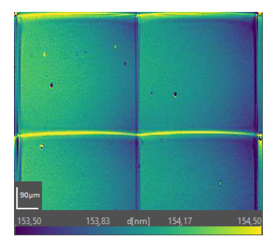
Similar to the first application example, the pixel-by-pixel analysis yielded images of the SiO₂ top-layer thickness (left) and again a map of the AOI-offset as a side product (right). The analysis reveals a gradient of SiO2 layer thickness across the microlenses. Compared to the first case study, edge effects at the outer borders between the lenses and the surrounding chromium apertures cause the thickness map to appear "less clean." However, the resulting thickness values across the individual lenses are not affected by these edge effects.
Summary
The imaging ellipsometer ep4 measures hyperspectral sets of micrographs of the sample's polarization properties. Computational modelling translates these data into layer-thickness micrographs.
This proof-of-concept study demonstrated unique layer-thickness measurements on microlenses with radii of curvature above 1 mm (ITO coating) and below 1 mm (SiO2 coating).
Imprint