


An Overview of Failure Analysis Methodologies Based on AFM
The importance of failure analysis in semiconductor manufacturing
Understanding failure modes, failure mechanisms, and root causes is crucial in the manufacturing of semiconductors and electronic devices. Determining the primary cause leading to a failure helps prevent it in the future, and therefore, improves product quality, reduces costs, and improves customer satisfaction. In the semiconductor manufacturing industry, failure analysis is related to the inspection and characterization of local defects on bare wafers, quality assessment of multi-stage processes, or function and performance analyses of finished devices. With the ever-progressing miniaturization of key functional parts of electronic devices, failure analysis is likewise becoming increasingly challenging due to the small dimensions and complicated structures of micro- and nano-scale devices. Accordingly, a powerful analysis yet easy-to-use tool is considerably needed to inspect, isolate, and characterize the defects. This whitepaper reviews some aspects of failure analysis methodologies in the fields of semiconductors and electronic device manufacturing. In particular, an overview of failure analysis based on Atomic force microscopy (AFM) will be introduced and reviewed.
Methodologies for failure analysis
Various tools have been widely adopted in semiconductor manufacturing for wafer defect inspection such as optical microscopy, laser-scattering inspection system, and electron microscopy. Although optical microscopy provides a quick view of a sample surface, imaging resolution is limited by Abbe's diffraction limit of about 200 nm for visible light. Wafer inspection based on laser-scattering yields higher resolution and defect detection sensitivity. However, several groups of defects (e.g., defect sites with very shallow depth) cannot be measured properly by this method due to weak light scattering. Electron microscopy methods are also facing a similar issue. Also, high-energy electron beam can modulate the structures of certain materials, hindering its application [1,2]. Furthermore, the results provided by imaging techniques based on electromagnetic waves are limited to two-dimensional maps, while in many cases three-dimensional data can provide a more comprehensive view of the defect. In addition, detailed information about a defect such as physical properties or chemical compositions should be fully understood to help identify the root cause.
To meet the aforementioned requirements for a failure analysis tool, scanning probe microscopy such as AFM has been introduced as an all-in-one solution that can provide multi-function analyses from surface topography to various physical and chemical properties, as denoted in Fig. 1. AFM measurement can be performed non-destructively with minimized sample preparation needs. Besides, AFM enables detailed characterization of micro- and nano-sized defects (e.g., dimensions, bump or pit type, and chemical composition), which is difficult to detect with conventional inspection tools. As a result, AFM is gaining traction as a valuable tool for defect analysis in high-volume semiconductor manufacturing. In the workflow of failure analysis, AFM can be used for fault isolation to locate and characterize the defect sites that lead to the failure [3]. However, widespread adoption of AFM is hindered by its relatively slow scan speed compared to conventional tools. Although informative, it typically takes several minutes to acquire an AFM image. For engineers working with bare wafers, the process of identifying nano-scale defects can be time-consuming when using conventional manual AFMs, hindering productivity, let alone throughput. Thus, it is important to have a solution to conduct automated failure analysis as well as provide production engineers with a versatile set of tools to perform in-depth investigations to find the root cause of defects on wafers.
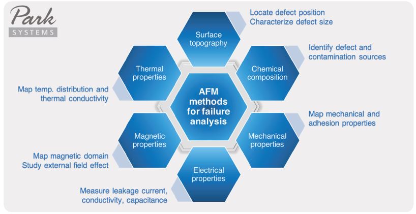
Fig. 1. Useful AFM methodologies for failure analysis.
Park Systems’ solutions for failure analysis
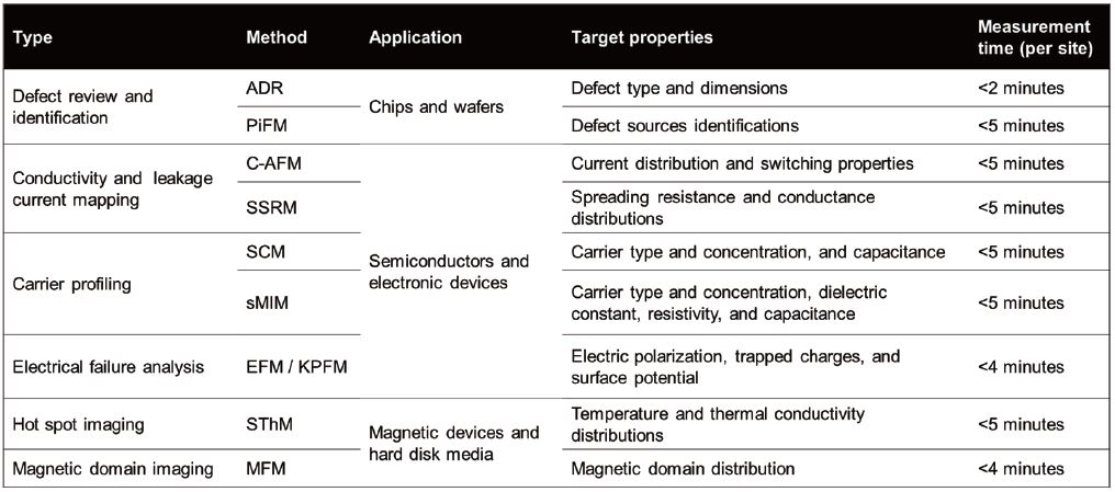
Table 1 summarizes AFM techniques that are widely used in various failure analysis studies for bare wafers, semiconductors, electronic devices, and magnetic devices. The versatility of AFM characterization is helpful in fault isolation and investigation of overall properties of the defect site to provide supportive information for root cause analysis. Park Systems offers a wide range of AFMs for both in-line and off-line measurements, enabling versatile applications from laboratory to industrial scales. Depending on a target property, users can switch to a corresponding AFM mode on the same tool, allowing various property measurements without redundant steps of switching among different systems and locating the respective defect again. This helps eliminate labor-intensive manual processes while maintaining high productivity.
Table 1. Summary of typically used AFM methods for failure analysis study. Note that various techniques within the scope of AFM are also available in addition to the methods mentioned in this document. Also, AFM scans can be combined with PinPoint™ operation for simultaneous measurement of surface, mechanical, and electrical properties.
Case study 1: Defect review and identification
To reduce labor-intensive manual processes of conventional AFM measurements, Park Systems has developed an automatic defect review (ADR) function which speeds up and improves the way defects are imaged and analyzed [2]. ADR AFM solutions can be implemented in various industries for bare wafers and hard disk media. Defect coordinates on a wafer, that have been obtained by inspection tools can be translated to the AFM for further analysis of the defect characteristics. Park Systems’ unique true Non-contact™ imaging mode allows non-destructive defect characterization with minimized wear of AFM tips, maintaining a high-resolution image in many consecutive measurements [4]. Non-contact imaging is especially useful to measure defects that are easily manipulated by high contact force of the tip. Fig. 2 shows the result of an ADR obtained using the Park Systems NX-Wafer on a 300 mm bare wafer. The AFM image of each defect site, along with detailed characteristics such as type, height, and size are automatically summarized in tabular form by the AFM operation software. The fully automated ADR solution has proven to be effective in the hard disk industry where the productivity of hard disk media failure analysis increased up to 10 folds compared to the manual method (manual searching for each defect site again when transferring the sample from the inspection tool) [2].
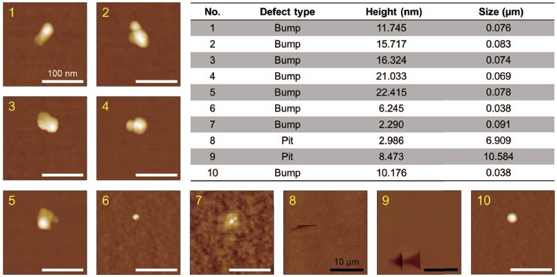
Fig. 2. Summary of ADR performed on a 300 mm bare wafer using Park Systems NX-Wafer. Automatic function yields an AFM image along with detailed characteristics of each defect site. White and black scale bars represent 100 nm and 10 μm, respectively.
In cases the defect source should be identified, the ADR function can be combined with Photo-induced force microscopy (PiFM) measurement [5]. PiFM allows for simultaneous morphology and chemical composition measurements of the defect site and can be used on a wide range of sample types from organic, inorganic, to biological materials. In failure analysis study, a high spatial resolution chemical adsorption map generated by PiFM gives detailed information on a defect or contaminant’s molecular fingerprint. When combined with the ADR function, detailed information of the defect site can be accumulated, assisting failure analysis engineers in identifying the root causes of faults or problems. Fig. 3 presents an example of PiFM measurement on a defect site of a bare wafer. After translating the defect coordinate from the inspection tool, PiFM spectroscopy measurement can be performed on the target defect site. Fig. 3(a) shows the PiFM spectroscopy measurement result obtained on the defect (red solid line) and on the substrate (black solid line). A significant difference between the spectra obtained on the defect and on the substrate indicates a discrepancy in chemical properties between them. By matching the PiFM spectra with an infrared spectral library, the defect’s chemical composition can be identified. In addition, PiFM can be operated in imaging mode at a selected wavenumber, allowing spatial distribution visualization of each chemical species across the defect surface, as shown in Fig. 3(b).
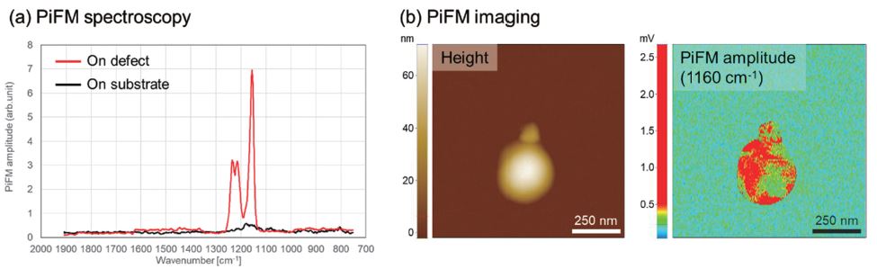
Fig. 3. Defect review and identification on a bare wafer using PiFM. Measurement is available in both (a) spectroscopy and (b) imaging modes. Experiment was performed using Park Systems NX-IR.
Case study 2: Leakage current measurement by C-AFM
Conductive AFM (C-AFM) measures the topography and current distribution across the sample surface. During scanning, a DC bias is applied to the sample, and the current flow through the tip-sample contact point is detected by a current amplifier. C-AFM allows visualization of heterogeneities in the conductivity of sample surface with current resolution as small as 0.1 pA. The versatility of current measurements allows the characterization of electrical properties across a wide range of materials from insulators to semiconductors and conductors. C-AFM is widely used in failure analysis to inspect leakage current, contact failure, and dielectric breakdown measurements of semiconductor devices [6,7]. Fig. 4 shows an example of leakage current measurement on a multi-layer necking device on a 300 mm wafer. The defect point was detected via current measurement at negative applied bias.
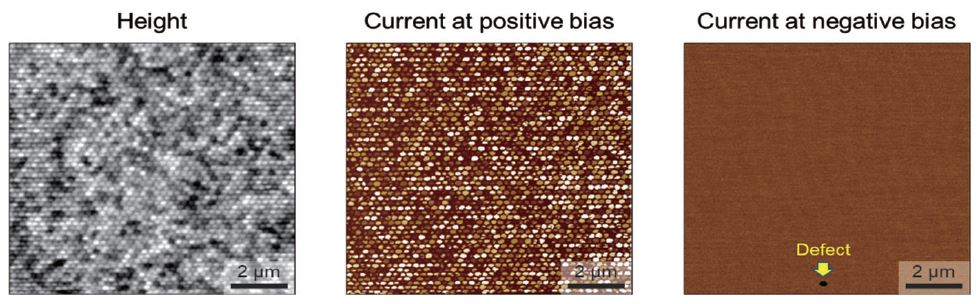
Fig. 4. Leakage current measurement on a multi-layer necking device on a 300 mm wafer using Park Systems NX-Wafer. A defect point was found with applied negative bias.
Case study 3: Inspecting SRAM device defect using SSRM
Scanning spreading resistance microscopy (SSRM) is an AFM technique in which a tip coated with a conductive material scans a biased sample surface and measures electrical properties such as current, conductance, or resistance of the sample, thus allowing probing of local doping profiles. Using a logarithmic amplifier, SSRM allows the measurement of samples consisting of different materials including insulators, semiconductors, and conductors. In ambient conditions, metal or semiconductor surfaces are typically covered with insulating oxide layers that potentially mask local electrical properties. SSRM utilizes a durable conductive diamond coated AFM tip to remove these oxide layers or any surface contamination, yielding high sensitivity and responsiveness to the current signal. To prevent re-oxidation or water adsorption on the sample surface while measuring, SSRM measurement is typically performed in vacuum or Ar/N2 gas conditions. Fig. 5 presents an example of defect inspection on a static random-access memory (SRAM) device using SSRM mode. The measurement was performed in a vacuum environment using the Park Systems NX-Hivac. The defect point on the device can be identified from irregularity in the resistance image. By considering the current and resistance criteria, the device can be evaluated as pass or fail the quality inspection test. Once the defect has been isolated, further tests can be conducted to find the cause of the failure.
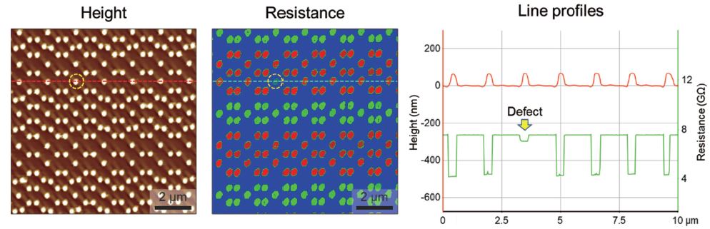
Fig. 5. SRAM device defect inspection based on SSRM mode. A defect point can be detected from irregularity in the resistance image. Measurement was performed in high vacuum using the Park Systems NX-Hivac.
Due to the nature of contact measurement, SSRM is more appropriate for hard materials such as silicon-based devices. For relatively soft materials, lateral force exerted during contact scan can damage the sample surface, causing artifacts in the measurement result. This issue can be minimized using PinPoint™ mode. PinPoint SSRM is an advanced version of conventional SSRM that allows simultaneous measurement of topography, electrical, and mechanical properties of the defect. This mode is performed in an approach-retract manner which is beneficial in minimizing lateral force exerted between the tip and sample as is in sliding contact, and hence, reducing damage to the sample and prolonging the lifetime of the AFM tip. Fig. 6 presents an example of PinPoint SSRM measurement. The resistance distribution of a Li-ion battery electrode was studied while simultaneously imaging surface topography and mechanical properties at the same time, which deepens the understanding of electrical properties in conjunction with the surface and mechanical properties of a material.
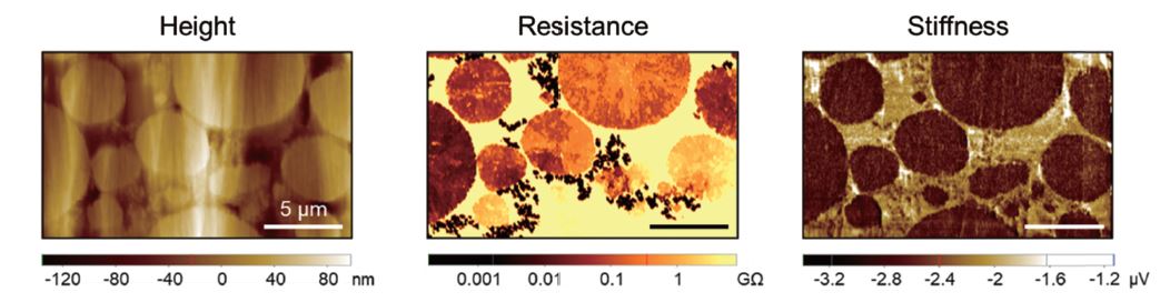
Fig. 6. Quality inspection of Li-ion battery electrode based on PinPoint SSRM mode. Measurement was conducted in high vacuum using the Park Systems NX-Hivac.
Case study 4: Monitoring silicon-on-insulator fabrication process using SCM
Scanning capacitance microscopy (SCM) measures spatial capacitance variations on semiconductors and thereby maps the carrier concentration and doping profiles in non-uniformly doped samples. SCM operates with a conductive material-coated AFM tip and a highly sensitive capacitance sensor in addition to regular AFM components. By applying an AC voltage while the conductive tip is in contact with the oxidized semiconductor sample, they form a metal-oxide-semiconductor (MOS) capacitor, with the tip and sample acting as electrodes. SCM can visualize nano-scale localized charges, trapped charges, and electronic defects, which is helpful for failure analysis in the semiconductor industry. For example, as the gate oxide of a MOS transistor gets thinner due to the reduction of overall device dimensions, problems and failures can occur, caused by charges trapped in the oxide layer during device operation. Presently, no other characterization tool is able to locally resolve the location of the failure and the electrical defects in two dimensions. Similarly, SCM is used to inspect the stored charges in the insulator layer of the metal-insulator-oxide-semiconductor heterostructure of the non-volatile memory devices.
Fig. 7 shows an example of dopant profile inspection during a semiconductor manufacturing process. The N-type polysilicon (N-poly) gate was implanted in a silicon-on-insulator (SOI) wafer as shown in the cross-section view of the sample structure. Then, the sample was annealed at high-temperature to repair lattice damage due to high-energy ion implantation and to activate the implanted ions [8]. SCM measurement results before and after annealing show how the surface morphology and doping characteristics change due to annealing, providing useful information for quality inspection and manufacturing process monitoring of the device.
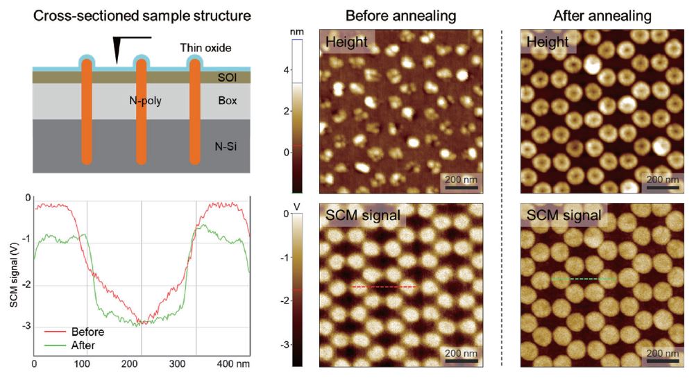
Fig. 7. Example of semiconductor manufacturing process monitoring based on SCM. Height images and dopant profiles comparisons reveal changes in morphology and doping characteristics of N-poly implant SOI device due to annealing. Measurement was conducted using Park Systems NX20.
While SCM provides information on the doping concentration and capacitance differences of semiconductor surfaces, it is not easy to convert those metrics into physical units. For applications that require quantitative characterization of electrical properties, scanning microwave impedance microscopy (sMIM) is a potential candidate [9]. sMIM uses microwave reflections from the tip-sample nanometric interaction to gather the local electrical properties of a sample, such as permittivity and conductivity. These two properties can then be converted to dielectric constant, capacitance, resistivity and dopant concentration (for semiconductors). sMIM is especially useful to characterize buried structures which are not accessible by conventional SCM measurement.
Case study 5: Thermal failure analysis of pole-tip recession by SThM
Scanning thermal microscopy (SThM) is an AFM technique developed for characterizing thermal properties. SThM uses a nanofabricated thermal probe to achieve high spatial and thermal resolution at the nano-scale. The measurement of thermal properties is available in temperature contrast mode (TCM) and thermal conductivity contrast mode (CCM). TCM measures temperature distribution while CCM probes spatial variation of thermal conductivity across the sample surface. The SThM mode of AFM allows simultaneous measurement of the surface morphology and thermal properties of a target sample. Failure analysis applications of SThM mainly focus on micro- and nano-scale thermal problems of semiconductor and electronic devices where conventional thermal analysis tools are not accessible.
Fig. 8 shows an example of TCM measurement on a pole-tip-recession of a hard disk drive head to study the temperature distribution as heating power is applied on either the writer or the reader. The SThM error image visualizes an increase in surface temperature due to applied heating power to the writer and reader. The peak temperature region as well as the heat flux of each component can be identified from the data. In combination with the device’s performance test, SThM data can provide supplementary information to help failure analysis and quality assurance engineers.
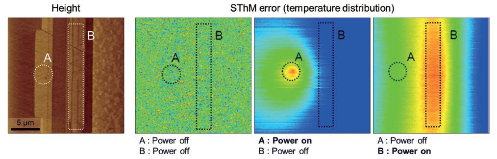
Fig. 8. SThM measurement on pole-tip-recession of a hard disk drive head. Writer (area A) and reader (area B) parts are marked on the height image. SThM error images show temperature distribution as heating power is applied to writer and reader. Measurement was performed using Park Systems NX20.
Case study 6: Characterizing magnetic sensor using MFM
Magnetic force microscopy (MFM) allows the measurement of the magnetic properties of various materials at the nano-scale. In this technique, a magnetic-sensitive material-coated tip scans the surface and maps the distribution and strength of magnetic domains on the sample. MFM can be applied to characterize, evaluate, and develop magnetic storage devices and magnetic recording components such as hard disk media, magneto-resistive heads, and magnetic sensors [10]. In addition to standard MFM imaging, Park Systems’ AFMs offer the possibility to apply external magnetic fields up to 6500 G in-plane and 2000 G out-of-plane, via a magnetic field generator to change the magnetic state of the sample. This allows magnetic characterization in various practical working conditions and environments of the device.
An example of MFM measurement on a magnetic device is presented in Fig. 9. A high-resolution optical microscopy equipped with the AFM allows a quick localization of the target scan area. After that, MFM measurement can be performed to probe the magnetic properties of the sample. The morphology and distribution of magnetic domains are visualized, providing information for quality inspection and failure analysis of the device.
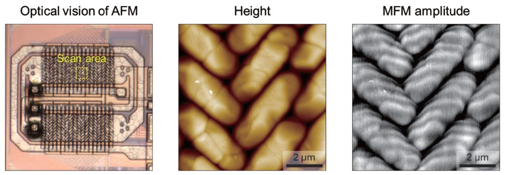
Fig. 9. MFM measurement on magnetic device performed using Park Systems NX20. High-resolution optical microscopy of the AFM allows coordinate mapping of the target scan area for MFM imaging.
Summary
This whitepaper introduces a few AFM methodologies that are helpful for failure analysis study and provides an overview of the capabilities and potentials of AFM as an instrument of choice for semiconductors and electronic device manufacturing. AFM allows non-destructive characterization of various surface, chemical, and physical properties of a target material. The automation of data acquisition and analysis along with advanced methodologies of Park Systems AFMs help accelerate mass adoption of AFM technology across various industrial applications.
References
[1] Q. Chen, C. Dwyer, G. Sheng, C. Zhu, X. Li, C. Zheng, Y. Zhu, Imaging Beam-Sensitive Materials by Electron Microscopy, Adv. Mater. 32 (2020) 1907619.
[2] R.Y.K. Yoo, Automated AFM Boosts Throughput in Automatic Defect Review, Micros. Today. 22 (2014) 18–23.
[3] J.M. Chin, V. Narang, X. Zhao, M.Y. Tay, A. Phoa, V. Ravikumar, L.H. Ei, S.H. Lim, C.W. Teo, S. Zulkifli, M.C. Ong, M.C. Tan, Fault isolation in semiconductor product, process, physical and package failure analysis: Importance and overview, Microelectron. Reliab. 51 (2011) 1440–1448.
[4] Park Systems Corp., Ultimate Resolution of Atomic Force Microscopy. https://www.parksystems.com/park-spm-modes/91-standard -imaging-mode/217-true-non-contact-mode.
[5] D. Nowak, W. Morrison, H.K. Wickramasinghe, J. Jahng, E. Potma, L. Wan, R. Ruiz, T.R. Albrecht, K. Schmidt, J. Frommer, D.P. Sanders, S. Park, Nanoscale chemical imaging by photoinduced force microscopy, Sci. Adv. 2 (2023) e1501571.
[6] C. Shin, K. Kim, J. Kim, W. Ko, Y. Yang, S. Lee, C.S. Jun, Y.S. Kim, Fast, exact and non-destructive diagnoses of contact failures in nano-scale semiconductor device using conductive AFM, Sci. Rep. 3 (2013) 2088.
[7] H. Kim, T. Park, S. Park, M. Leem, W. Ahn, H. Lee, C. Lee, E. Lee, S.-J. Jeong, S. Park, Y. Kim, H. Kim, Ultrathin monolithic HfO2 formed by Hf-seeded atomic layer deposition on MoS2: Film characteristics and its transistor application, Thin Solid Films. 673 (2019) 112–118.
[8] R. Nipoti, H.M. Ayedh, B.G. Svensson, Defects related to electrical doping of 4H-SiC by ion implantation, Mater. Sci. Semicond. Process. 78 (2018) 13–21.
[9] A. Melgarejo, N. Antoniou, Electrical Characterization using Scanning Microwave Impedance Microscopy,. https://www.parksystems. com/learning-center/nano-academy/articles/3884-electrical-characterization-using-scanning-microwave-impedance-microscopy.
[10] M. Winter, F.J.T. Goncalves, I. Soldatov, Y. He, B.E.Z. Céspedes, P. Milde, K. Lenz, S. Hamann, M. Uhlarz, P. Vir, M. König, P.J.W. Moll, R. Schlitz, S.T.B. Goennenwein, L.M. Eng, R. Schäfer, J. Wosnitza, C. Felser, J. Gayles, T. Helm, Antiskyrmions and their electrical footprint in crystalline mesoscale structures of Mn1.4PtSn, Commun. Mater. 3 (2022) 102.