


-
Hafnia ScanningSpreadingResistanceMicroscopy Tin disulfide LightEmiting high_resolution Wafer Polarization Spincast Lateral_Force_Microscopy Austenite Moire NUSNNI FM_SKPM temp_control Varistor Vacuum Jason Modulus CrossSection CalciumHydroxide ring shape oxide_layer KevlarFiber Graphite Fiber self_healing Memory Pinpoint Strontium atomic_layer PyroelectricDetector Ferrite EFMAmplitude self-assembled_monolayer LowDensityPolyethylene
Report image
If you found this image unacceptable, please let us know. We will review your report and take action if we determine this image is really unacceptable.
Polymer patterns on Si (2/2)
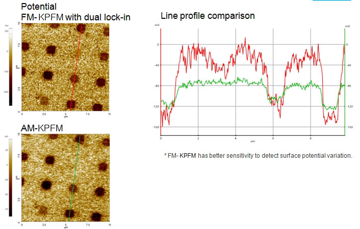
Scanning Conditions
- System: NX10
- Scan Mode: KPFM
- Cantilever: NSC36Cr-Au (k=1N/m, f=90kHz)
- Scan Size: 10μm×10μm
- Scan Rate: 0.2Hz
- Pixel: 512×256