


Fei Hui
Fei Hui is currently a postdoctoral fellow in Technion-Israel Institute of Technology, she received her PhD degree from the University of Barcelona in 2018. During her PhD, Dr. Hui was a visiting scholar at Massachusetts Institute of Technology (USA) for 12 months, where she learned chemical vapor deposition two-dimensional (2D) materials (e.g. hexagonal boronnitride, graphene) on different substrates (i.e. Cu, Pt, Fe and Ni). She also received the Researcher Mobility Grant from Royal Society of Chemistry, which supported her studies at the University of Cambridge (UK) for 6 months. In the Cambridge Graphene Center, she learned how to synthesize graphene oxide thin films and, more interestingly, how to cover nanoprobes with thin films of this material via spray technique. She has published over 40 research papers (11 papers are as first-author) on top journals of Nature Electronic, Advanced Functional Materials, ACS Applied Materials and Interfaces, 2D Materials (amongothers), and with more than 811 citations indicated by Google Scholar (https://scholar.google.com/citations?user=Ht0HvKYAAAAJ&hl=en&oi=ao). She has applied for two international patents, and one of them (cost-effective fabrication of ultra-durable graphene coated nanoprobes) attracted around $1 million investment.
1. Please summarize the research you do and explain why it is significant?
My research topic is the development of two-dimensional (2D) materials based electronic devices. We are aiming to integrate 2D materials (e.g. hexagonal boron nitride, graphene or molybdenumdisulfide) into electronic devices (e.g. memristors or field effecttransistors). Due to the atomic thin layer and extraordinary properties (e.g.high thermal and electrical conductivity, flexibility and transparency) of 2D materials, it allows us to design miniaturized devices, which exhibit some exotic performances that conventional transition metal oxides (e.g. HfO2)-based devices do not show. More specifically, I firstly synthesis monolayer ormultilayer 2D materials using chemical vapor deposition (CVD) methodology. After growth I used several techniques to analyze the quality of these materials, mainly Raman Spectroscopy and cross-sectional transmission electron microscopy(X-TEM), but the technique that provided me best results was conductive atomicforce microscopy (CAFM). Using this technique, I explored the dielectric properties of hexagonal boron nitride (h-BN) and graphene oxide (GO), including tunneling current, charge trapping, trap-assisted tunneling, stress-induced leakage current, dielectric breakdown and resistive switching (RS). I also used these 2D materials to fabricate memristive devices, and analyzed them using aprobestation connected to a semiconductor parameter analyzer (working in different atmospheres).
2. How might your research be used?
In my work, I employed a scalable CVD technique to synthesis large size of 2D materials, which allow us to fabricate high-yield electronic devices and study their device-to-device variability. Moreover, this methodology is more compatible with and useful for the industry than single/few devices fabricated by mechanical exfoliation. In our previous work, we have proved that h-BN can be used as a RS medium and the metal/h-BN/metal devices showed both volatile and non-volatile RS behaviors, enabling the emulation of a range of synaptic-like behavior, including both short- and long- term plasticity. Therefore, our research would accelerate the use of 2D materials for building future wafer-scale and high-density electronic memories and/or artificial neural networks.
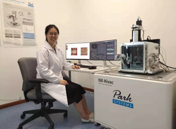
3. What features of Park AFM are the most beneficial and why?
Park AFM system is a powerful tool that provides us with more accurate and reliable information under different conditions (ambient and vacuum conditions), which is extremely important for the research field of nanoscience. First of all, the true non-contact mode allows us to acquire the topographic information, such as the wrinkles of 2D materials or some tiny particles, without the damage of probes and surface modification of specimens. Second,the image/position drift is negligible, we can perform spectroscopy measurements (e.g. current vs. voltage, force vs. distance) at specific location or in a matrix pattern and then go back to them exactly. Moreover, the navigation and the software interface are quite user-friendly, which save us much more time.
4. Why is the Park AFM important for your research?
This Park NX-Hivac system is able to simultaneously perform four tasks that are essential to study RS reliably: i) measure currents in tapping mode (to avoid premature tip wearing and material damage), ii)measure high currents from picoamperes to miliamperes in both polarities by using a logarithmic preamplifier (to monitor the set/reset transitions insitu), iii) measure in high vacuum up to 10-6 torr (to avoid localanodic oxidation and unwanted moisture-related reactions), and iv) measure at high temperatures up to 600 ºC (not only to study reliability, but also to evaporate all water molecules on the materials after pumping the vacuum). The need of these four features to reliably measure RS at the nanoscale is extensively described in the book (Conductive Atomic Force Microscopy:Applications in Nanomaterials, ISBN: 978-3-527-69978-0, Wiley-VCH Weinheim,Germany, 2017) edited by Prof. Mario Lanza, who is a leading expert in CAFM science, and there is no other equipment in the world that can carry out all these actions simultaneously. The use of this tool will be a high advantage compared to other groups.