


Electrochemical Atomic Force Microscopy: In Situ Monitoring of Copper Electrodeposition on Gold Surface
John Paul Pineda, Mario Leal, Gerald Pascual, Byong Kim, Keibock Lee Park Systems Inc., Santa Clara, CA USA
INTRODUCTION
In recent years, understanding electrochemical processes such as electrodeposition (also known as electroplating) has become important for various technologies and sciences including microelectronics, nanobiosystems, solar energy conversion, and chemistry among others, due to its wide range of applications [1, 2]. Electrodeposition is a conventional process that utilizes electrical current through an electrolyte solution to modify surface properties, either chemical or physical, to make the material suitable in certain applications. This process reduces the cations of a desired material and deposits particles onto the conductive substrate surface of the material [3]. This technique is commonly done to enhance electrical conductivity, improve corrosion resistance and heat tolerance, and/or to make products more aesthetically appealing. A good deposition mainly depends on the substrate surface morphology [4]. Thus, a technique that can measure these characteristics and monitor the process at nanoscale is greatly needed. There are several methods that were employed for this surface characterization. Examples include scanning electron microscopy (SEM) and scanning tunneling microscopy (STM). These techniques allow measurement of structures on the nanoscale, however, some of them are ex situ, some typically require high vacuum environments, and others are not applicable in monitoring continually changing processes because of high consumption of time for image acquisition [2, 5]. To overcome these shortcomings, electrochemistry (EC) combined with atomic force microscopy (commonly known as EC-AFM) was introduced. This technique allows users to perform in situ imaging and visualization of changes in sample surface morphology being studied under certain electrochemical environments at nanoscale [6].
In this study, the deposition and dissolution of copper nanoparticles onto a gold surface was successfully demonstrated and clearly observed in situ using a Park NX10 AFM and current-voltage (CV) curves was simultaneously acquired using a potentiostat during the experiment.
Experimental
AFM Head and Tip
A liquid probehand shielded with glass was used instead of a conventional probehand to allow measurements in liquid. A NANOSENSORS PointProbe® Plus-Contact (PPP-CONTSCPt) cantilever (nominal spring constant k = 0.2 N/m and resonant frequency f = 25 kHz) coated with platinum and mounted on a Teflon chip carrier was used in the experiment. A platinum coated cantilever was selected to maintain beam intensity when the tip is immersed in the solution. Moreover, the tip was mounted on a Teflon chip carrier to protect the EC cell from other unwanted electric signals that could affect the conditions of the electrolyte solution.
EC Cell Setup
An EC Cell manufactured by Park Systems was used in the experiment. The cell is made of polychlorotrifluoroethylene (PCTFE) to ensure chemical stability. A sample is mounted in the cell with a top cover and sealed with a thin silicon O-ring to securely prevent leaking. The working electrode (WE) that was used was a thin film made of gold (111) evaporated onto a mica surface while the reference electrode (RE) and counter electrode (CE) were silver chloride (AgCl) and platinum-iridium (Pt-Ir) wires. The 3 electrodes were connected on a Solartron Modulab ECS XM potentiostat. The aqueous solution contained 0.1 mM CuSO4 in 50 ml of 0.01mM H2SO4. Sulfuric acid was added to the solution for stabilization and to prevent the formation of copper precipitate.
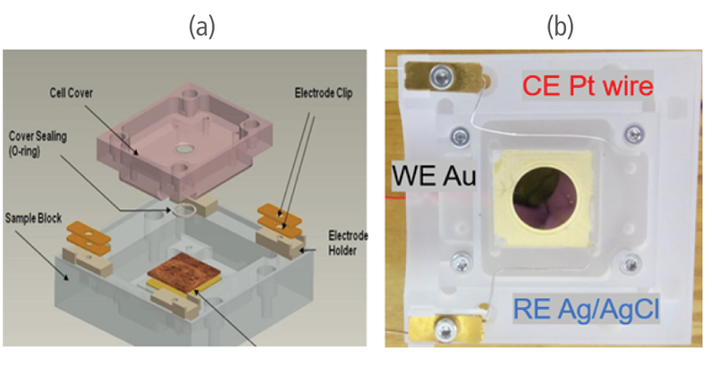
Figure 1. C(a) Overall structure of the EC Cell and (b) its actual setup in the study.
EC-AFM Experiment Conditions
The deposition and dissolution of the copper nanoparticles in gold (111) thin films was monitored using a Park NX10 system. Reference images of the gold surface were acquired in ambient air and in liquid condition without introducing any chemical reaction to serve as a point of comparison for the sample surface before and after the experiment. The images were acquired via AFM using non-contact mode. After obtaining the reference image in-liquid, the 3 electrodes were connected into the potentiostat. The CE and RE were bent before immersion in the liquid solution to make a good contact and prevent saturation of the signal. The AgCl electrode was utilized as the RE since a chloride solution was not used. Furthermore, Pt-Ir electrode was selected as the CE since this material is chemically stable and would not contaminate the solution.
In EC-AFM, the WE is the sample surface where the electrodeposition process takes place and the CE is where the electric current is expected to flow. The EC cell with the electrodes in place is like an electronic circuit and the main function of CE is to close the circuit’s current loop. The RE is used as a fixed reference point and serves to provide feedback for maintaining a stable voltage in the solution. An electric field was supplied in the WE to transmit electrons to the ions in the solution so that chemical reactions will take place. The type of chemical reaction depends on the amount of voltage supplied (either positive or negative voltage) in the solution. In this study, cyclic voltammetry was applied to the EC cell to know the oxidation and reduction peaks of the solution. After determining the threshold voltages where oxidation and reduction occur, linear sweep voltammetry was applied to deposit and dissolve copper nanoparticles onto and from the gold (111) WE surface. Two scans were performed with -0.2 V to -0.4 V to cover the entire surface of the gold with copper nanoparticles. On the other hand, 4 scans were performed with -0.2 V to 0 V to completely dissolve the copper nanoparticles back into the solution.
Results and Discussion
Figure 2 shows the CV curve obtained during cyclic voltammetry. 4 complete cycles of oxidation and reduction process (redox process) were selected in obtaining the curve. The result implies that these processes are reversible depending on the amount of potential applied on the solution. The deposition of copper begins when -0.2 V was applied on the cell and the highest reduction state takes place when -0.4 V was applied. The result can be interpreted that increased negative potential applied into the cell will increase the magnitude of the copper being deposited onto the WE. On the other hand, the dissolution of copper begins when the voltage is 0 V and the highest oxidation state takes place in application of 0.1 V. The magnitude of the copper dissolved in the gold surface will increase as increasing positive potential applied into the cell. The CV curve also shows that in -0.1 V, the solution is in neutral state wherein no chemical reaction occurs.
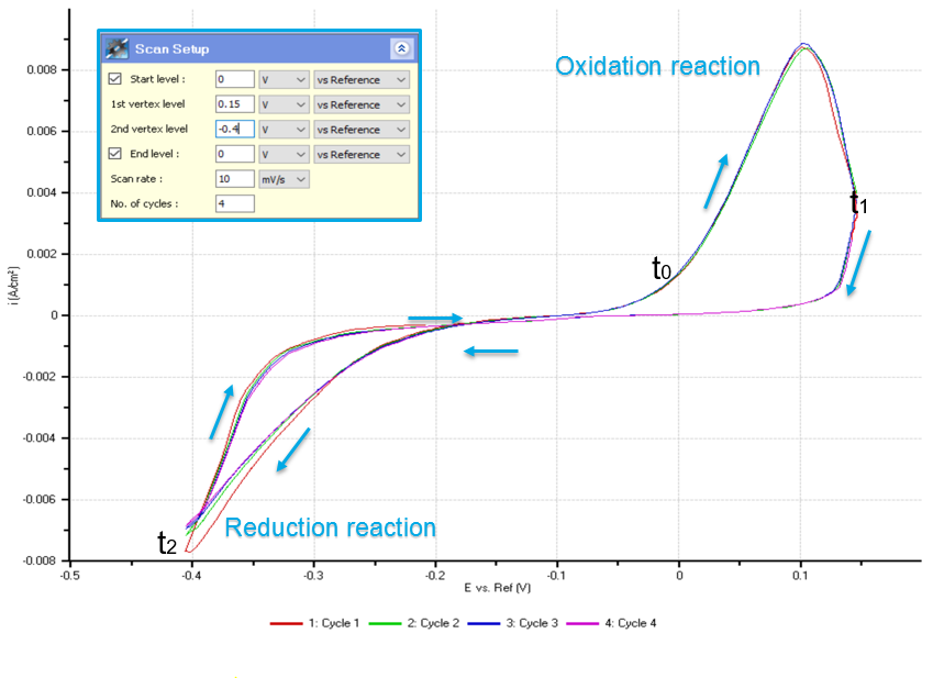
Figure 2. Cyclic voltammogram. The negative peaks demonstrate the reduction reaction state where copper is deposited onto the sample (WE) surface. The positive peaks demonstrate the oxidation state where copper is dissolved from the sample (WE) surface.
Figure 3 (a) and (b) revealed that the 5 μm by 5 μm scanned region (in ambient air) and 1 μm by 1 μm scanned region (in liquid condition) of the gold (111) surface is made of individual grains that are crystalized. These images show no foreign particles are present on the surface prior to introducing electrochemical reactions in the solution.
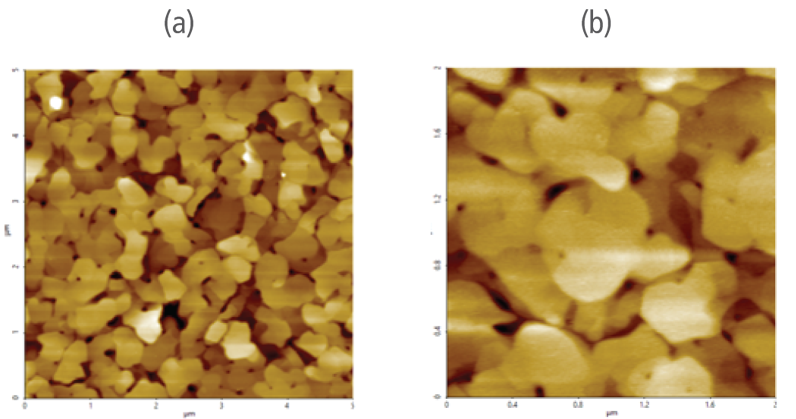
Figure 3. Pre-electrochemical reaction reference AFM images of the sample (WE) gold (111) surface (a) acquired in air and (b) in liquid.
The redox process was confirmed using AFM and voltages were applied using linear sweep voltammetry. Figure 4(b) and 4(d) shows the CV curves acquired by applying voltages from -0.2 V to -0.4 V. The current density decreases as more negative voltage was applied. This phenomenon demonstrates that a reduction reaction is occurring. Figure 4(a) and 4(c) confirmed this process wherein the images clearly show that copper nanoparticles were successfully deposited on the gold (111) surface. Copper nanoparticles were quantified using Park XEI software developed by Park Systems which marked each detected particles with different colors and numbers. The detection method used by the software was upper threshold grain detection. In this method, a threshold value is set and particles whose heights are smaller than the threshold value are not detected. In this experiment, 5.5 nm was used as the threshold value to quantify the copper particles. Since the gold (111) surface is composed of individual grains with various heights, most of the copper nanoparticles were deposited on lower regions with height values smaller than the threshold value and were not detected. Figure 4(a) shows the image acquired during the first deposition test. The number of particles detected by this test was approximately 7 with a mean area value of 2 nm². In addition, there are particles deposited on lower regions with smaller height values that were not detected by the image analysis software. Furthermore, 199 particles were detected on a second test with a mean area value of 36 nm² as shown in Figure 4(b). The data shows that the number of particles deposited on the second test was 28 times in size than the number detected in the first test and were found in a larger area covering nearly the entirety of the gold (111) surface.
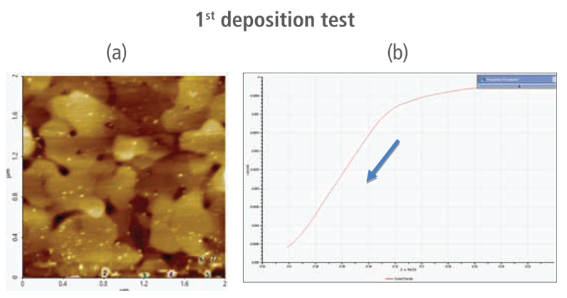
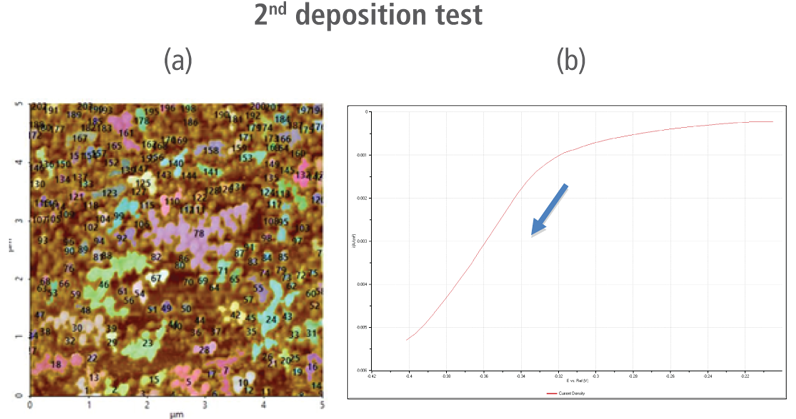
Figure 4. (a) and (c) AFM images acquired on the first and second deposition tests, (b) and (d) CV curves acquired using linear sweep voltammetry with voltages from -0.2 V to -0.4 V on the first and second deposition tests.
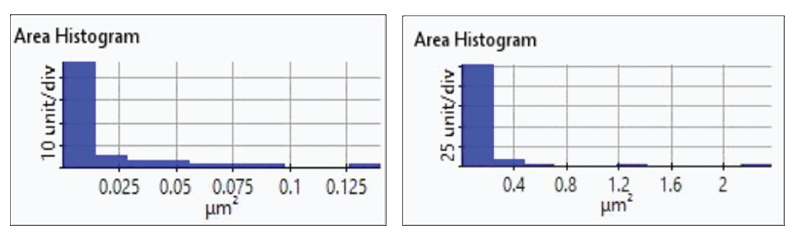
Figure 5. Histogram plots of particles area distribution on the first (left)and second (right) deposition test
The CV curves acquired by applying reverse voltages from -0.2 V to 0 V during the dissolution process showed that current density increases as more positive voltage was applied. This phenomenon demonstrates that an oxidation reaction occurred. The AFM images acquired in this process confirmed that the number of copper particles deposited on the gold surface decreases after dissolution tests were performed. Figure 6(a) shows the image acquired in the first dissolution test. The number of particles detected on the test was 180 with mean area value of 37 nm². The particles detected on this test are slightly fewer with smaller mean area value compared to particles detected in the second deposition test. Almost similar results were obtained in second dissolution test wherein the number of particles detected were 181 but with a smaller mean area value of 24 nm². On the other hand, the results on third dissolution test showed a significant decrease in the number of particles detected around 19 with mean area value of 7 nm². Lastly, the fourth and final dissolution test dissolved nearly all copper nanoparticles including those deposited on the lower region of the gold (111) surface as shown in Figure 6(h).
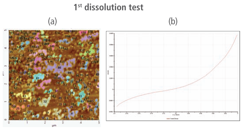
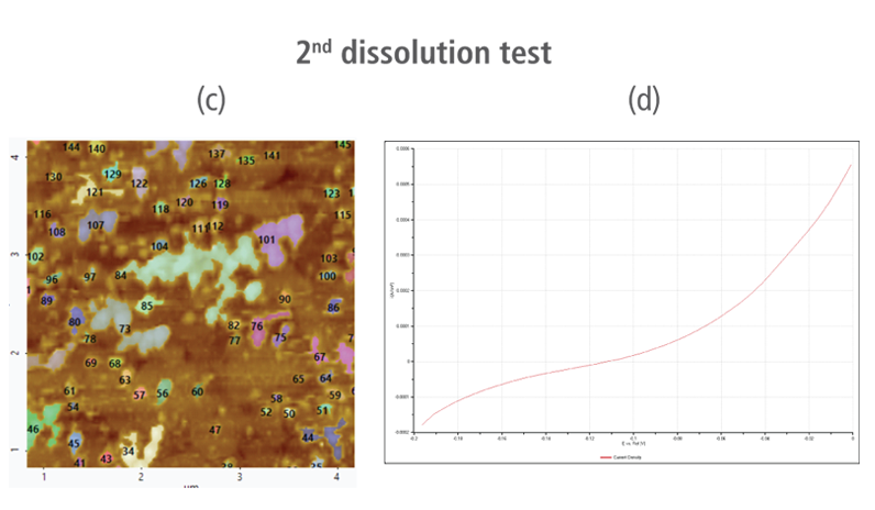
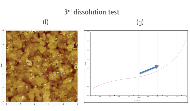
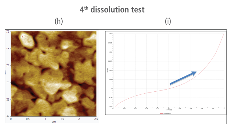
Figure 6. (a), (c), (f), and (h) AFM images acquired on first to fourth dissolution tests, (b), (d), (g) and (i) CV curves acquired using linear sweep voltammetry with voltages from -0.2 V to 0 V on first to fourth dissolution tests.
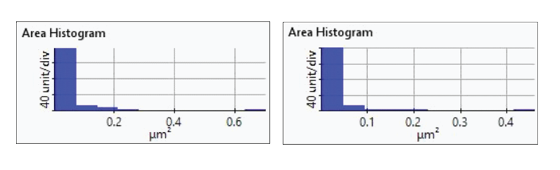
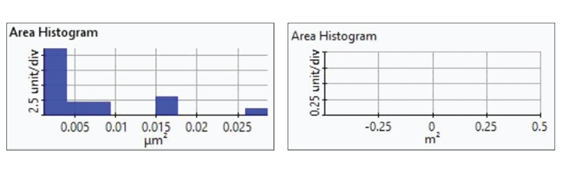
Figure 7. Histogram plots of particle area distributions from the first(upper-left), second (upper-right), third (bottom left), and fourth(bottom-right) dissolution tests.
CONCLUSIONS
Here we demonstrate the use of EC-AFM for in situ monitoring of morphological changes of samples that are undergoing electrochemical processes. The deposition and dissolution of the copper nanoparticles on a gold (111) thin film surface were successfully performed by applying suitable voltages suggested by a CV curve acquired via cyclic voltammetry. The data from the deposition process demonstrate that the magnitude of copper deposited on the gold (111) surface increases tremendously from a first to a second round of deposition via reduction. On the other hand, the results on a third (of four) round of dissolution via oxidation showed a significant decrease in the number of copper nanoparticles deposited remaining on the gold (111) surface. Overall, the technique described in this study will successfully provide researchers nanoscale information to aid in producing significant insights to understanding electrochemical processes.
References
[1] Dryhurst G., et al. Application of Electrochemistry in the Studies of the Oxidation Chemistry of Central Nervous System Indoles. Chem. Rev. 1990
[2] Schlesinger M., et al. Modern Electroplating. Fifth edition, pg. 27
[3] Saidin N., et al. ELECTRODEPOSITION: PRINCIPLES,APPLICATIONS AND METHODS
[4] Popoola A., et al. Effect of some process variables on zinc coated low carbon steel substrates. Scientific Research and Essays Vol. 6(20), pp. 4264-4272, 19 September, 2011
[5] Smith T., et al. Electrochemical SPM Fundamentals and Applications.
[6] Reggente M., et al. Electrochemical atomic force microscopy: In situ monitoring of electrochemical processes.