


Electrostatic artifacts in magnetic force microscopy measurement
Introduction
Over the past decades, Atomic force microscopy (AFM) has been intensively involved in nanoscale research and development. Despite being widely used, understanding AFM data is sometimes cumbersome, especially for a new AFM user. The extraordinary sensitivity of AFM to various forces and effects makes it not only a versatile research tool but also prone to different sources of artifacts. Such artifacts can arise from incorrect system and experimental setups, or complex material behaviors.
This study illuminates the example of electrostatic artifacts and how to avoid them when conducting Magnetic force microscopy (MFM). MFM is a variant of AFM which is used to characterize the magnetic properties of a sample on a nanometer scale. Here, interactions between the tip and sample are generally governed by three major forces: short-range van der Waals forces, and long-range magnetic and electrostatic forces. MFM utilizes the difference in distance dependence of these forces to separate the van der Waals forces (∝r-6)) from the magnetic and electrostatic forces (∝r-2 ) by performing a dual pass scan. For that, each scan line is measured twice: the topography is scanned in the first pass at close proximity where short-ranged van der Waals forces dominate the interactions. The tip is then lifted in the second pass and retraces the topography. At larger distances of 50-500 nm, the short-range van der Waals interactions become minimal, and magnetic or electrostatic forces govern the tip-sample interaction. However, it is difficult to distinguish between the magnetic and electrostatic forces during conventional MFM measurements due to their similar force ranges [1]. As a consequence, the superposition of magnetic and electrostatic forces can distort the actual MFM signal. Moreover, additional artifacts can originate from optical interference that occurs when the superluminescent diode (SLD) beam reflected off the back of the cantilever interferes with the beam reflected from the sample surface, creating a fringe or wave pattern in the obtained AFM images [2].
A combined kelvin probe force microscopy–magnetic force microscopy (KPFM–MFM) technique was used to perform real-time compensation electrostatic interaction between the tip and sample during the measurement [1,3,4]. Fig. 1 shows a schematic diagram of the dual pass KPFM–MFM measurement. Similar to standard MFM, the sample is scanned twice to collect an artifact-free MFM signal. In the first pass, the non-contact mode is used to scan the surface topography using the first lock-in amplifier exclusively for topography feedback. In the second pass, the tip will retrace the topography obtained from the first scan while adding a constant lift distance above the sample surface. By doing this, the van der Waals force can be separated, leaving electrostatic and magnetic forces contributions. To separate the electrostatic force, a Sideband KPFM [5] measurement which can detect the electrostatic force between the tip end and the sample is performed simultaneously in the second pass. In this case, the second and third lock-in amplifiers are used to obtain the contact potential difference between the tip and sample based on Sideband KPFM mode. As a result, electrostatic contributions can be compensated in real-time by applying a nullifying VDC bias. This leaves the magnetic contribution unaffected that can be measured by detecting the amplitude or phase shift of the tip modulation from the first lock-in amplifier.
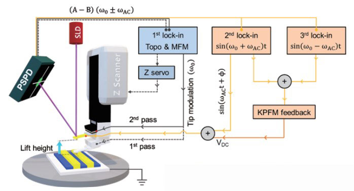
Figure 1. Schematic diagram of KPFM–MFM measurement. In Sideband KPFM, an electrical excitation lower than the resonance frequency (ωAC≪ω0 ) is applied to the cantilever. 2nd and 3rd lock-in amplifiers are used to decouple right (ωAC+ω0 ) and left (ωAC-ω0 ) sidebands from deflection signal (A-B).
Measurements and results
The effects of electrostatic contribution on MFM results were studied for cases of homogeneous and heterogeneous distributions of electrostatic forces across the sample surface. To simulate the two cases, Ni–Cr–Mo alloy and MoSe2–WSe2 heterostructure samples were prepared, respectively. The samples were mounted onto a non-magnetic sample holder to avoid magnetic signal interference by the magnetic sample holder that is typically used in AFM. An automatic AFM (FX40, Park Systems) equipped with a concentrated SLD beam was employed using a cobalt alloy coated tip (PPP-MFMR, Nanosensors) that provides magnetic and electrostatic sensitivities. Automatic beam alignment of the FX40 positions the SLD beam spot at an optimized location on the cantilever to avoid artifacts due to optical interference.
Figure 2 summarizes examples of KPFM–MFM measurements on a sample that has a uniform surface potential due to a homogeneous distribution of electrostatic force across the surface. For comparison, a standard MFM measurement was also conducted at the same location using the same tip. From the MFM phase images in Figs. 2(a) and 2(b), and line profiles comparison, it was found that the electrostatic force had no significant effect on the observation of magnetic properties of the sample. As confirmed by the potential image in Fig. 2(b), a uniform distribution of the surface’s electrostatic force is expected to exhibit a constant contribution to the measured data and therefore does not affect magnetic contrast among domains on the sample surface. In other words, despite the existence of electrostatic force, the relative difference between the magnetic domains of the sample is not affected. Hence, the electrostatic contribution can be omitted in this case. However, electrostatic force compensation is still required in cases where a quantitative measurement of magnetic properties is needed.
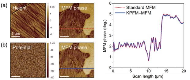
Figure 2. Measurement results on Ni–Cr–Mo alloy sample. MFM phase signals are collected based on standard MFM (a) and combined KPFM–MFM (b) modes. The potential image in (b) shows no difference in surface potential across the sample surface. Line profiles are shifted along Y axes for comparison.
The effect of electrostatic contributions on a sample with a heterogeneous surface potential is visualized in Fig. 3. Here, the surface potential difference between MoSe2–WSe2 flakes and the SiO2/Si substrate induced artifacts in MFM measurements as expected. Clear differences in MFM phase images as well as in the line profiles were observed after removing the electrostatic contribution. The standard MFM measurement in Fig. 3(a) exhibited gradients around the flake along with a strong contrast between the flakes and underlying substrate, while these features were strongly suppressed in the KPFM–MFM data (Fig. 3(b)). This suggests that the actual magnetic properties of the MoSe2–WSe2 sample are negligible. These results emphasize how the actual magnetic signal is distorted by variations in surface potential across the surface. In this circumstance, without consideration of the electrostatic contributions, one would accept the standard MFM measurement result as magnetic characteristics of the sample, leading to an erroneous conclusion on the result.
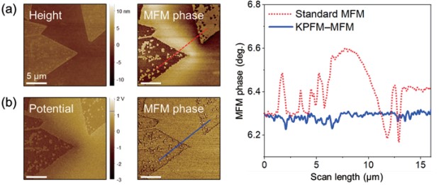
Figure 3. Measurement results on MoSe2–WSe2 heterostructure sample. MFM phase signals are collected based on MFM alone (a) and combined KPFM–MFM (b) modes. The potential image in (b) shows variation in surface potential across the sample surface. Line profiles are shifted along Y axes for comparison.
Summary
This study demonstrates the effects of electrostatic contribution on MFM measurements. It was found that the MFM signal can be distorted if the sample has potential variation across the surface, while the effect was insignificant on a sample that has a uniform surface potential. The combined KPFM–MFM measurement was used to perform real-time compensation of surface potential difference between tip and sample during scanning. It is suggested that the electrostatic properties of the sample should be carefully considered to improve the accuracy of magnetic properties measurement using the AFM.
References
1. M. Jaafar, O. Iglesias-Freire, L. Serrano-Ramón, M.R. Ibarra, J.M. de Teresa, A. Asenjo, Distinguishing magnetic and electrostatic interactions by a Kelvin probe force microscopy-magnetic force microscopy combination., Beilstein J. Nanotechnol. 2 (2011) 552–560.
2. P. Eaton, K. Batziou, Artifacts and Practical Issues in Atomic Force Microscopy BT - Atomic Force Microscopy: Methods and Protocols, in: N.C. Santos, F.A. Carvalho (Eds.), Springer New York, New York, NY, 2019: pp. 3–28.
3. D. Martínez-Martín, M. Jaafar, R. Pérez, J. Gómez-Herrero, A. Asenjo, Upper Bound for the Magnetic Force Gradient in Graphite, Phys. Rev. Lett. 105 (2010) 257203.
4. O. Kazakova, R. Puttock, C. Barton, H. Corte-León, M. Jaafar, V. Neu, A. Asenjo, Frontiers of magnetic force microscopy, J. Appl. Phys. 125 (2019) 60901.
5. Park Systems Corp., A Comparative Study of Atomic Force Microscopy between AM KPFM and Sideband KPFM: Principles and Applications, n.d. https://parksystems.com/images/media/appnote/AppNote-61_sideband-KPFM_A-comparative-study.pdf.