


Correlating the electrochemical response of 2D materials to their thickness
Marc Brunet Cabréa, Aislan Esmeraldo Paivaa,
Matej Velickýb, c, d, Paula E. Colavitaa, Kim McKelveya, e
a Trinity College Dublin (Ireland) b University of Manchester (United Kingdom) c Cornell University (United States) d J. Heyrovský Institute of Physical Chemistry (Czech Republic) e Victoria University of Wellington (New Zealand)
This Application Note is based on a publication by Marc Brunet Cabré et al. “Electrochemical kinetics as a function of transition metal dichalcogenide thickness”, Electrochimica Acta 393, 139027 (2021), https://doi.org/10.1016/j.electacta.2021.139027
Introduction:
Two-dimensional (2D) transition metal dichalcogenides (TMDCs) display unique electronic, chemical, and mechanical properties [1]. These properties facilitate the use of 2D TMDCs as active materials for electrochemical and -catalytic applications [2 – 4], where they can serve as electrodes for Li-ion batteries [5] or as electrocatalysts for the hydrogen evolution reaction (HER) [3, 6 – 9]. However, the preparation of 2D TMDCs often results in heterogeneous sample morphologies that feature flakes of various sizes and thicknesses. Here, particularly variations in the flake thickness i.e., the number of TMDC layers, can change the material’s electronic structure and electrochemistry substantially [2, 10, 11]. The correlation of certain TMDC thicknesses to their respective electrochemical activity requires real-space characterization techniques with sub-nanometer height resolution to distinguish the number of layers and highly localized electrochemical measurements.
Scanning probe microscopy (SPM) can meet these requirements by combining the sub-nanometer height sensitivity of the atomic force microscopy (AFM) topography with local electrochemistry measurements available in scanning electrochemical cell microscopy (SECCM). SECCM can map the electrochemical activity with a spatial resolution of tens to hundreds of nanometers by limiting the measurement area to a nanodroplet at the end of a nanopipette, which serves as electrochemical cell [12–14]. Therefore, SECCM facilitates localized electrochemistry measurement at the area of interest, without exposing the rest of the surface to the electrolyte. The combination of SECCM data with the complementary AFM topography allows correlating the electrochemical activity with the thickness of the TMDC flakes.
In our publication, we used Park Systems’ SECCM (Figure 1 A) and AFM capabilities to compare the electrochemistry of monolayers, bilayers, and trilayers of the four different 2D TMDCs MoS2, MoSe2, WS2, and WSe2 on gold. Therefore, we identified suitable imaging areas via the optical microscope of the Park NX10, analysed the electrochemical response from a [Ru(NH3)6]3+/2+ redox couple on the samples via SECCM (Figure 1 B and C) and resolved the layer numbers of the measurement spots in subsequent AFM topography measurements. This allowed the direct correlation of sample thickness with the electrochemical activity.
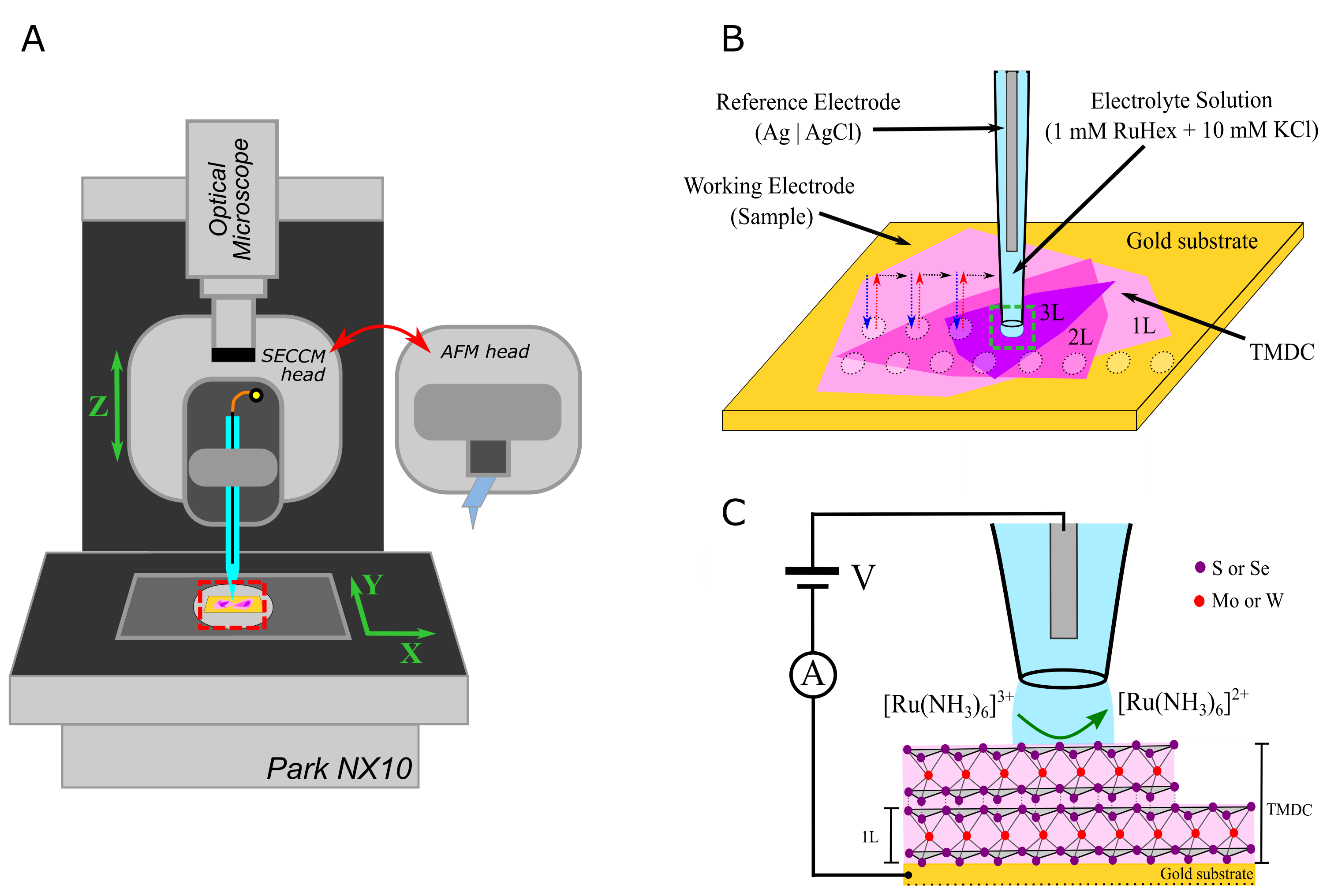
Fig. 1. (A) Schematic of the Park NX10 experimental setup, featuring a SECCM probe and an exchangeable AFM probe head (B) Schematic of the SECCM nanopipette probe mapping the electrochemical response of the TMDC surface. (C) Schematic of the nanodroplet-based electrochemical cell (located at the end of a SECCM probe), showing the electrochemical reaction taking place at TMDCs surface, the TMDC structure, and the electrical contact with the Au substrate. Images are reproduced with permission.[16] Copyright 2021, Electrochimica Acta
Experimental:
TMCD layers (MX2, M = Mo or W and X = S or Se) were mechanically exfoliated from bulk crystals and deposited onto Au substrates serving as bottom-contact for electrical connection.
Optical, AFM, and SECCM measurements were performed on the NX10 by Park Systems, South Korea. AFM images were obtained in non-contact mode (NCM) with a PPP-NCHR cantilever type (force constant = 42 N/m, resonance frequency = 330 kHz, Nanosensors). For the SECCM measurements, nanopipettes from single-barrel borosilicate capillaries with 300 – 600 nm aperture radius were filled with 1 mM [Ru(NH3)6]3+ solution in 10 mM aqueous KCl. An Ag/AgCl reference electrode was inserted into the nanopipette. The nanopipette was positioned on the surface using the NX10 optics. Linear sweep voltammograms (LSV) were recorded on a predefined grid with a distance of 1.5 μm between individual measurement spots. To avoid damage to the nanopipette probe, a spectroscopy mode was used (Figure 1 B). Here, the probe retracts prior to the lateral movement between measurement spots and approaches each spot until contact between the droplet and the surface is established at a threshold current of 5 pA. In contact, LSVs were recorded by sweeping the potential between +0.2 V to -0.8 V at a speed of 1 V/s.
Results and Discussion:
The optical microscopy function of the NX10 AFM was used to identify suitable measurement areas that feature TMDCs flakes with different layer numbers (1L-3L) prior to SECCM characterization, as shown in Fig. 2 A. To resolve the exact layer number of the TMDC at the SECCM measurement spots, AFM step height profiles were extracted from topography images obtained after the SECCM experiments (Fig. 2 B). The profiles of 1L/2L and 2L/3L MoSe2 are displayed in Fig. 2 C and 2 D. In agreement with previous AFM measurements on MoSe2 [15], we determined monolayer thickness of 0.81 nm and 0.78 nm. Salt residues from the SECCM allowed correlating the electrochemical response of each measurement spot to the exact layer thickness. Moreover, the diameter of the salt residue measured via AFM facilitated an estimate of the droplet/surface contact area during the SECCM measurements.
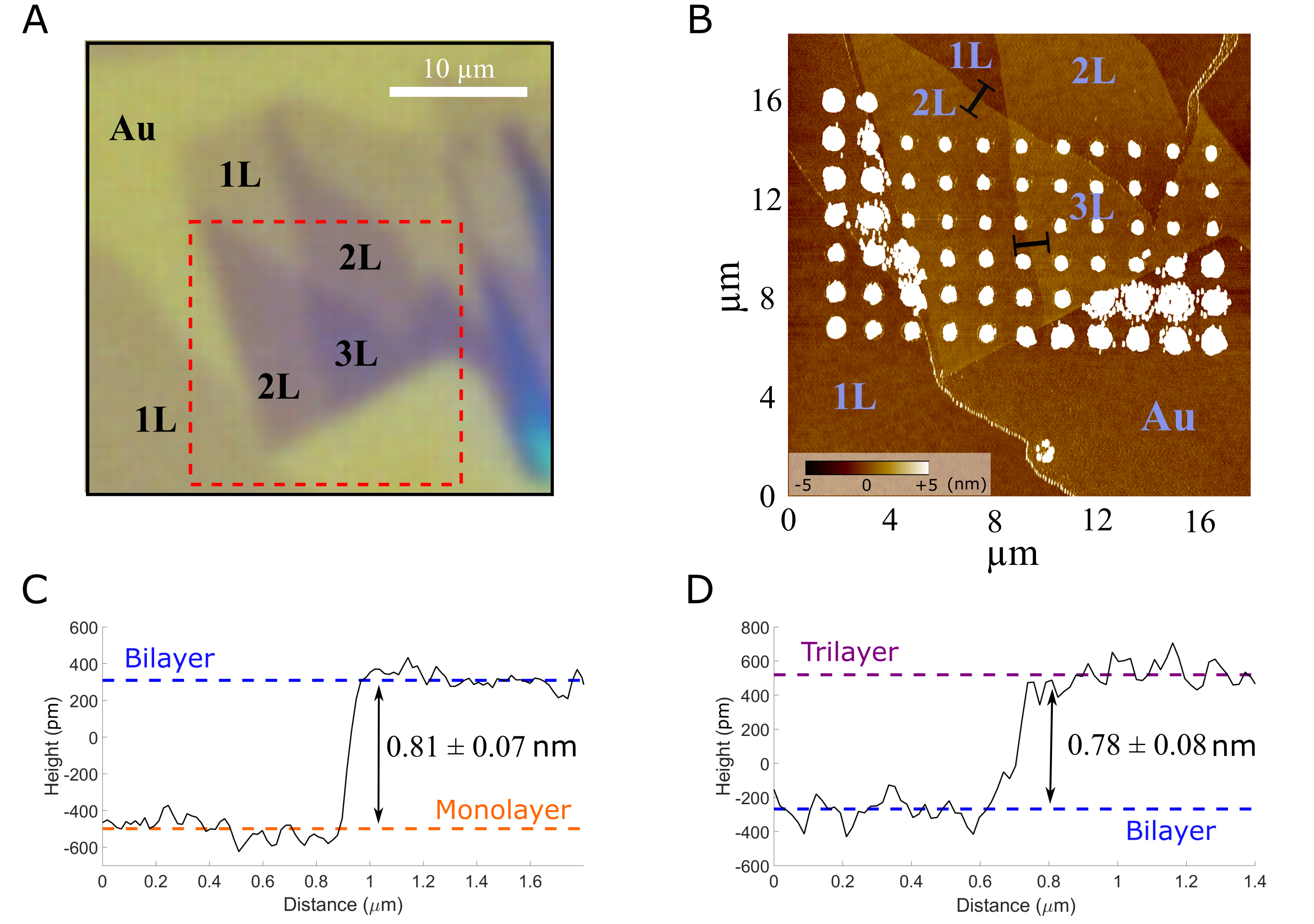
Fig. 2. (A) Optical image of MoSe2 crystals with differing number of layers. (B) AFM image of a region depicted by the red rectangle in part (A). The AFM was taken after the SECCM measurements and therefore revealed the electrolyte residues at the areas of contact between the droplet and surface. (C) and (D) line profiles of 1L/2L and 2L/3L boundaries, respectively, taken from areas shown by black lines in (B). Step height was calculated as the difference of the average terrace height (dashed coloured lines). Images are reproduced with permission.[16] Copyright 2021, Electrochimica Acta
LSVs on 1L, 2L, and 3L WS2 in Fig. 3 A, B, and C clearly show that the electrochemical behaviour depends on the number of TMDC layers. The [Ru(NH3)6]3+ reduction is more facile on monolayer WS2 and the onset potential increases as the number of layers increases. To quantify the observed electrochemical response, we modelled the diffusional transport of [Ru(NH3)6]3+/2+ and the electron transfer kinetics at the sample surface. Finite element method allowed to generate a simulated electrochemical response. By adjusting the kinetic parameter kmax, the simulation was matched to each individual experimental LSV, which facilitates an estimation of the apparent kmax for each layer number (kmax.nL for n L), as shown in Fig. 3 A - C for WS2 based on the corresponding AFM measurement in Fig. 3 D. We found that an increase in layer number leads to a decrease in the reaction rate, as highlighted in Fig. 3 E. In our publication, we furthermore performed the same analysis on 1L, 2L, and 3L of MoS2, MoSe2, and WSe2 to find that all investigated TMDC materials show a slowing down of the kinetics with the increasing number of layers. [16]
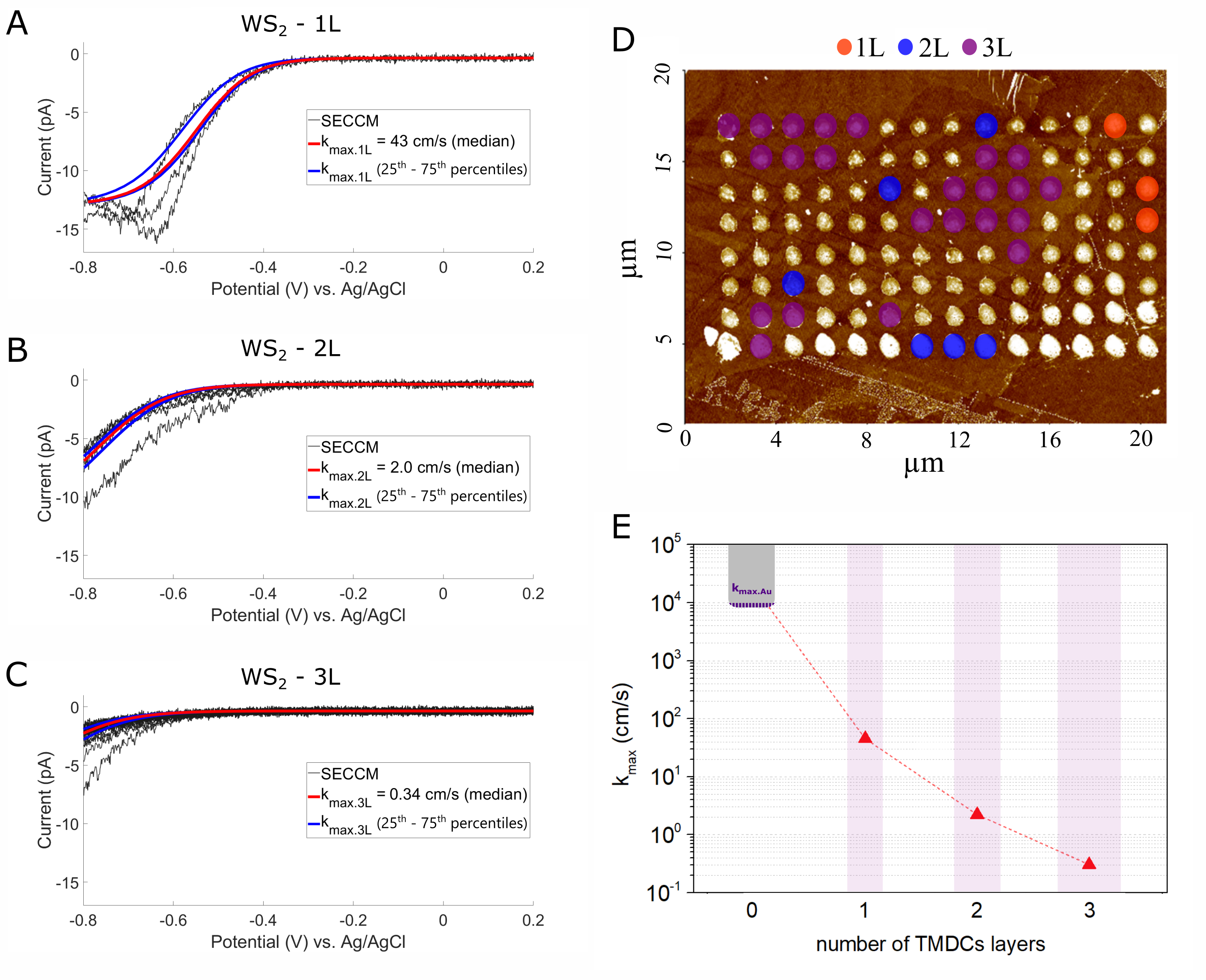
Figure 3: (A), (B), and (C) LSVs of [Ru(NH3)6]3+ reduction on 1L, 2L, and 3L respectively from the points shown in Figure 3 B (black traces). Simulated response corresponding to the median fitted in red and simulated response corresponding to 25th and 75th percentiles of kmax fitting in blue. (D) Color-coded surface type assignment over the AFM image showing SECCM point grid on WS2. (E) Values determined from fitting simulation to experimental data for different layer thickness of WS2. Solid points correspond to each value and the dashed line is displayed to guide the eye. Images are reproduced with permission.[16] Copyright 2021, Electrochimica Acta
Conclusion:
In this application note, we summarized the findings of our recent publication “Electrochemical kinetics as a function of transition metal dichalcogenide thickness”, Electrochimica Acta 393, 139027 (2021), https://doi.org/10.1016/j.electacta.2021.139027. To investigate the electrochemical response of 2D TMDC materials in dependence of their layer number we correlated the AFM sample height to a SECCM grid measurement with the outer sphere redox couple [Ru(NH3)6]3+/2+ performed on a Park NX10 AFM. We found that the electrochemical response on the different numbers of stacked layers changes significantly, with increasing reaction rates on decreasing layer numbers on all tested TMDCs.[16]
References:
[1] S. Manzeli, D. Ovchinnikov, D. Pasquier, O. V. Yazyev, A. Kis, 2D transition metal dichalcogenides, Nat. Rev. Mater. 2 (2017) 17033–17048, DOI: https://doi.org/10.1038/natrevmats.2017.33
[2] M. Velický, P. S. Toth, From two-dimensional materials to their heterostructures: An electrochemist's perspective, Appl. Mater. Today 8 (2017) 68–103, DOI: https://doi.org/10.1016/j.apmt.2017.05.003
[3] X. Chia, A. Y. S. Eng, A. Ambrosi, S. M. Tan, M. Pumera, Electrochemistry of Nanostructured Layered Transition-Metal Dichalcogenides, Chem. Rev. 115 (2015) 11941–11966, DOI: https://doi.org/10.1021/acs.chemrev.5b00287
[4] M. Chhowalla, H. S. Shin, G. Eda, L. J. Li, K. P. Loh, H. Zhang, The chemistry of two-dimensional layered transition metal dichalcogenide nanosheets, Nat. Chem. 5 (2013) 263–275, DOI: https://doi.org/10.1038/nchem.1589
[5] T. Stephenson, Z. Li, B. Olsen, D. Mitlin, Lithium ion battery applications of molybdenum disulfide (MoS2) nanocomposites, Energy Environ. Sci. 7 (2014) 209–231, DOI: https://doi.org/10.1039/C3EE42591F
[6] Z. Zhu, H. Yin, C. T. He, M. Al-Mamun, P. Liu, L. Jiang, Y. Zhao, Y. Wang, H. G. Yang, Z. Tang, D. Wang, X. M. Chen, H. Zhao, Ultrathin Transition Metal Dichalcogenide/3d Metal Hydroxide Hybridized Nanosheets to Enhance Hydrogen Evolution Activity, Adv. Mater. 30 (2018) 1–7, DOI: https://doi.org/10.1002/adma.201801171
[7] Q. Fu, J. Han, X. Wang, P. Xu, T. Yao, J. Zhong, W. Zhong, S. Liu, T. Gao, Z. Zhang, L. Xu, B. Song, 2D Transition Metal Dichalcogenides: Design, Modulation, and Challenges in Electrocatalysis, Adv. Mater. 33 (2020) 1907818, DOI: https://doi.org/10.1002/adma.201907818
[8] L. Lin, P. Sherrell, Y. Liu, W. Lei, S. Zhang, H. Zhang, G. G. Wallace, J. Chen, Engineered 2D Transition Metal Dichalcogenides—A Vision of Viable Hydrogen Evolution Reaction Catalysis, Adv. Energy Mater. 10 (2020) 1903870, DOI: https://doi.org/10.1002/aenm.201903870
[9] Q. Lu, Y. Yu, Q. Ma, B. Chen, H. Zhang, 2D Transition‐Metal‐Dichalcogenide‐Nanosheet‐Based Composites for Photocatalytic and Electrocatalytic Hydrogen Evolution Reactions, Adv. Mater. 28 (2016) 1917–1933, DOI: https://doi.org/10.1002/adma.201503270
[10] M. Velický, G. E. Donnelly, W. R. Hendren, S. McFarland, D. Scullion, W. J. I. Debenedetti, G. C. Correa, Y. Han, A. J. Wain, M. A. Hines, D. A. Muller, K. S. Novoselov, H. D. Abruna, R. M. Bowman, E. J. G. Santos, F. Huang, Mechanism of Gold-Assisted Exfoliation of Centimeter-Sized Transition-Metal Dichalcogenide Monolayers, ACS Nano 12 (2018) 10463–10472, DOI: https://doi.org/10.1021/acsnano.8b06101
[11] Y. Yu, S. Y. Huang, Y. Li, S. N. Steinmann, W. Yang, L. Cao, Layer-Dependent Electrocatalysis of MoS2 for Hydrogen Evolution, Nano Lett. 14 (2014) 553–558, DOI: https://doi.org/10.1021/nl403620g
[12] M. E. Snowden, A. G. Güell, S. C. S. Lai, K. McKelvey, N. Ebejer, M. A. O’Connell, A. W. Colburn, P. R. Unwin, Scanning Electrochemical Cell Microscopy: Theory and Experiment for Quantitative High Resolution Spatially-Resolved Voltammetry and Simultaneous Ion-Conductance Measurements, Anal. Chem. 84 (2012) 2483–2491, DOI: https://doi.org/10.1021/ac203195h
[13] N. Ebejer, A. G. Güell, S. C. S. Lai, K. McKelvey, M. E. Snowden, P. R. Unwin, Scanning Electrochemical Cell Microscopy: A Versatile Technique for Nanoscale Electrochemistry and Functional Imaging, Ann. Rev. Anal. Chem. 6 (2013) 329–351, DOI: https://doi.org/10.1146/annurev-anchem-062012-092650
[14] N. Ebejer, M. Schnippering, A. W. Colburn, M. A. Edwards, P. R. Unwin, Localized High Resolution Electrochemistry and Multifunctional Imaging: Scanning Electrochemical Cell Microscopy, Anal. Chem. 82 (2010) 9141–9145, DOI: https://doi.org/10.1021/ac102191u
[15] J. C. Shaw, H. Zhou, Y. Chen, N. O. Weiss, Y. Liu, Y. Huang, X. Duan, Chemical vapor deposition growth of monolayer MoSe2 nanosheets, Nano Res. 7 (2014) 511–517, DOI: https://doi.org/10.1007/s12274-014-0417-z
[16] M. Brunet Cabré, A. Esmeraldo Paiva, M. Velický, P. E. Colavita, K. McKelvey, Electrochemical kinetics as function of transition metal dichalcogenides thickness, Electrochimica Acta. 393 (2021) 139027, DOI: https://doi.org/10.1016/j.electacta.2021.139027