


Surface Potential Characterization of Two-Dimensional Materials through Back-Gate Voltage Biases
Seok-Ju Kang 1, Jong Yun Kim 1, Jaekyung Kim 2, Oh Hun Gwon 1, and Young-Jun Yu 1
1 Department of Physics, Chungnam National University, Republic of Korea
2 Park Systems Corp., Suwon, Republic of Korea
Introduction
Two-dimensional (2D) materials including semi-metallic graphene, semiconducting transition metal dichalcogenides (TMDs), and insulating hexagonal boron nitride (hBN), have been studied in recent years as electrically or photonically innovative materials. Among various applicable electronic devices, from the specific perspective of memory devices, non-volatile floating gate transistors have been widely researched for high-performance information storage devices.1,2 Moreover, the van der Waals (vdW) heterostructures of 2D materials have been further investigated for artificial synaptic emulators for neuromorphic computing systems.2,3 In this regard, the typical 2D materials-based floating gate memories are constituted from TMDs, hBN, and graphene as a semiconductor, tunnel barrier, and floating gate, respectively. Furthermore, it is very important to understand the primitive factors, which affect the charge trapping or detrapping behavior in a deep potential well. Therefore, a comprehensive investigation of the 2D material’s properties at energy levels is imperative to demonstrate the fast and low-powered flash memories.
For this purpose, the floating gate memory structure was prepared with mechanically exfoliated thin MoS2, hexagonal boron nitride (hBN), and multilayer graphene (MLG). Afterwards, we examined the work functions of the respective layers depending on the back-gate voltages using a kelvin probe force microscopy (KPFM) apparatus.
Materials and Methods
Transfer process for 2D materials
Flakes of each 2D material (MoS2, hBN, and MLG) were exfoliated onto a rectangular piece of cured polydimethylsiloxane (PDMS) by mechanical exfoliation with the standard scotch tape method4. Subsequently, we transferred the exfoliated 2D materials slowly onto the SiO2/p++Si substrate in the order of MoS2/hBN/MLG stacking. During the transfer process, the 2D flakes on PDMS were precisely aligned with the intended position on the target substrate by a micro-manipulator and were then brought into contact.
KPFM measurement with gate bias
KPFM measurements were obtained using a commercial atomic force microscope system (NX10, Park Systems Corp.) at room temperature in air. An Au-coated cantilever with a Cr sublayer on an n-type silicon material (Mikromash corp., spring constant: 1 N/m, resonance frequency: 90 kHz) was used as the conductive tip. During the observation of the surface potential data, an AC voltage amplitude of ~2 V and a frequency of 17 kHz were applied to a conductive probe. The surface potential was obtained by applying a feedback DC voltage (VDC) with a lock-in amplifier to cancel the electrostatic force between the Au-coated tip and the sample generated by the AC voltage (VAC) applied to the tip.5, 6 To investigate the effect of the back-gate bias (VBG) during KPFM analysis, we observed changes in surface potential while maintaining a constant VBG bias by sequentially applying a VBG of 0 V or 40 V. The morphology and surface potential data were later analyzed using Park Systems XEI software to retrieve numerical information from the measured mapping images.
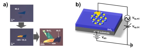
Figure 1. a) Optical microscope images of the transfer process for 2D vdW heterostructures (MoS2/hBN/MLG).
b) Representative schematic of the KPFM setup with applied VBG for the 2D materials on a SiO2/Si substrate. The scale bars in a) are 20 µm.
Results and Discussion
To fabricate multi-stacked 2D heterostructures, the MLG, hBN, and MoS2 were transferred sequentially to a SiO2/p++Si substrate, as shown in Fig. 1a. The transferred MLG, hBN, and MoS2 are adopted to fulfill the roles of semi-metal, wide bandgap insulator, and semiconductor, respectively. The multi-stacked heterolayers were characterized through the KPFM setup with applied VBG to examine the surface potential variances of each 2D layer depending on the back-gated voltages, as presented in Fig. 1b. In this system, the Fermi levels or work-functions could be changed under the back-gate bias.
The multi-stacked heterostructure was constructed successfully as observed by optical microscopy and presented in Fig. 2a. The surfaces of the layers remained largely uncontaminated during the transfer process, such that the topographic and electrical information were not affected.
From the height profile of a line-scan indicated in the AFM morphology image, the thicknesses of MoS2, hBN, and MLG could be calculated to approximate values of 6.9, 60.5, and 12.0 nm, respectively. The overall stacking structure with each thickness value for the three layers is presented in Fig. 2d.
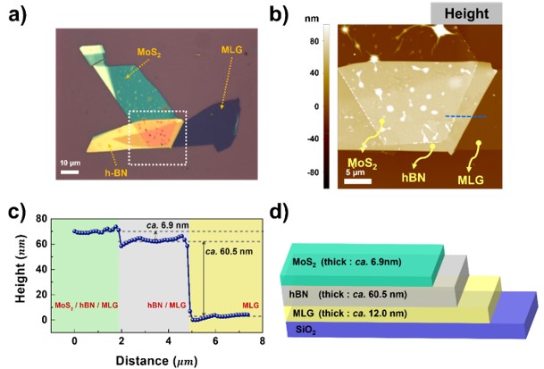
Figure 2. a) Optical image of MoS2/hBN/MLG heterostructure. The scale bar in a) is 10 µm.
b) A surface topography image of a). The scale bar in b) is 5 µm.
c) The height profile of the line-scan (blue dash line) indicated in b).
d) The stacked multi-layer heterostructure on a SiO2 substrate with the respective thickness values as measured in c).
To verify the different behavior of MoS2-based floating gate memory devices, we measured the surface potentials and the work-functions of MoS2, hBN, and MLG using a KPFM system where VBG was applied as shown in Figs. 3a, b and 3d, e, respectively.
The KPFM measurements yielded the contact potential difference (VCPD) between the Au-coated AFM tip and the sample and we then obtained the following relationship.

where WFsample and WFtip are the work functions of the sample and tip, respectively, and e is the electronic charge.
Since our vdW heterostructure is floating on a SiO2 substrate, we used the contact potential and the work function of MLG as standard points. As a result, the contact potential or work function differences between the various multi-stacking layers and MLG could be described as the equations below.
For the hBN/MLG stacking layers, 
For the MoS2/hBN/MLG stacking layers,

The work-function difference (ΔWFH-G or ΔWFM-G) was calculated through equation (3) for hBN or equation (5) for MoS2. As seen in Figs. 3c, f, while applying a VBG bias of 40 V, the Fermi energy levels of each stacked 2D material (MoS2, and hBN) were shifted higher from the initial positions (VBG = 0 V) with respect to the work-function level of MLG. In the case of ‘VBG = 0 V’, the work-function differences for the two surfaces of hBN/MLG (ΔWFH-G and MoS2/hBN/MLG (ΔWFM-G) layers are ca. -171.9 meV and ca. -265.8 meV, respectively. Thus, the Fermi levels are positioned lower than the MLG work function level. However, in the case of ‘VBG = 40 V’, the work-function differences for the two surfaces of hBN/MLG (ΔWFH-G) and MoS2/hBN/MLG (ΔWFM-G) layers are ca. 89.0 meV and ca. 125.2 meV, respectively. Hence, the Fermi levels are positioned higher than the MLG work function level.
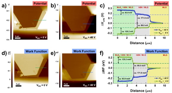
Figure 3. KPFM images of multilayer vdW heterostructure (MoS2/hBN/MLG): a, b) surface potential and d, e) work function in the case of VBG = 0 V (a, d),
or VBG = 40 V (b, e). Line-scan profiles of potential (c), and work function (f), which are indicated in a, b), and d, e) respectively. The scale bars in a, b, d, e) are 5 µm.
Due to the different work-function level behaviors depending on the VBG bias, the MLG layer can be efficiently charged with electrons or holes by tunneling.
To summarize the results, under the VBG condition of 0 V, electrons in the MLG layer could migrate more easily to the MoS2 layer by overcoming the barrier of the hBN layer. Contrary to this, for the VBG condition of 40 V, the MLG layer would be convenient to obtain electrons from the MoS2 layer with a reduced energy barrier between MoS2 and hBN layers.
Conclusion
For the study of the charge transfer behavior through the hBN insulating layer, the back-gated KPFM mode was utilized as a method to investigate the surface potential properties of 2D materials when back-gate voltages of 0 and 40 V were applied. Through the method of the back-gated KPFM, we scrutinized the cause of the charging and discharging behavior of the graphene layers embedded in the structure of a MoS2/hBN/MLG on SiO2/p++Si substrate. Ultimately, the back-gated KPFM method could be widely employed to characterize the device operation mechanisms of non-volatile floating gate memories, memtransistors, and various other electrically functional devices.
References
[1] Bertolazzi, S.; Bondavalli, P.; Roche, S.; San, T.; Choi, S. Y.; Colombo, L.; Bonaccorso, F.; Samori, P., Nonvolatile Memories Based on Graphene and Related 2D Materials. Adv Mater 2019, 31 (10), e1806663.
[2] Seo, S.; Lee, J. J.; Lee, H. J.; Lee, H. W.; Oh, S.; Lee, J. J.; Heo, K.; Park, J. H., Recent Progress in Artificial Synapses Based on Two-Dimensional van der Waals Materials for Brain-Inspired Computing. Acs Appl Electron Ma 2020, 2 (2), 371-388.
[3] Yi, S. G.; Park, M. U.; Kim, S. H.; Lee, C. J.; Kwon, J.; Lee, G. H.; Yoo, K. H., Artificial Synaptic Emulators Based on MoS2 Flash Memory Devices with Double Floating Gates. ACS Appl Mater Interfaces 2018, 10 (37), 31480-31487.
[4] Huang, Y.; Sutter, E.; Shi, N. N.; Zheng, J.; Yang, T.; Englund, D.; Gao, H. J.; Sutter, P., Reliable Exfoliation of Large-Area High-Quality Flakes of Graphene and Other Two-Dimensional Materials. ACS Nano 2015, 9 (11), 10612-20.
[5] Yu, Y. J.; Choe, J. H.; Kim, J. Y.; Gwon, O. H.; Choi, H. K.; Choi, J. S.; Kim, J. H.; Kim, J. S.; Kim, J. T.; Shin, J. H.; Choi, Y. K., Gate-tuned conductance of graphene-ribbon junctions with nanoscale width variations. Nanoscale 2019, 11 (11), 4735-4742.
[6] Yu, Y. J.; Zhao, Y.; Ryu, S.; Brus, L. E.; Kim, K. S.; Kim, P., Tuning the graphene work function by electric field effect. Nano Lett 2009, 9 (10), 3430-4.