


Intrinsic electrical characterization of two-dimensional transition metal dichalcogenides via scanning probe microscopy
Yuanyuan Shi1, Jill Serron1, Benjamin Groven1, Albert Minj1, Pierre Morin1 and Thomas Hantschel1
1IMEC, Kapeldreef 75, 3001 Leuven, Belgium
*The following application note is based on ACS Nano publication, 2021 15, 6, 9482–9494.
Publication Date: May 27, 2021.
Introduction
In a conventional planar silicon field effect transistor (FET), the gate controllability becomes weaker when its lateral dimension becomes smaller than the transistor thickness, which results in adverse short-channel effects, including leakage current, saturation of the carrier mobility in the channel, channel hotcarrier degradation, and time-dependent dielectric breakdown. Hence, the transistor body thickness needs to be reduced to ensure efficient electrostatic control from the gate. Due to the atomic thickness and dangling bond-free surface of twodimensional (2D) materials, theoretical studies have shown that particularly 2D transition metal dichalcogenides (TMDs) can outperform Si as the channel material, enable the atomic-level scaling, excellent electrostatic gate control, decrease off-state power consumption and further extend Moore’s Law.[1-6]
Suitable techniques to characterize the intrinsic physical and electrical properties of as-deposited 2D materials, are a key link between the quality of as-deposited 2D materials and the performance of 2D materials-based electronic devices. This link can help us to better understand, control and improve the performance of 2D materials-based devices. However, techniques for analyzing the intrinsic electrical properties of as-deposited 2D materials on the nanoscale without any transfer and patterning process are limited.
In this application note, scanning probe microscopy (SPM) is used to investigate the intrinsic electrical properties of as-deposited 2D TMDs. Conductive atomic force microscope (C-AFM) is performed directly on the surface of as-grown 2D materials without any patterning. C-AFM allows correlating the electrical conductivity of as-grown 2D materials to their topography, thereby linking the electrical properties of 2D materials to their physical properties such as layer thickness, etc. With all of this, C-AFM gives us comprehensive information of as-deposited 2D materials and helps us to evaluate the impact of these intrinsic properties on 2D materials-based nanoelectronics.
Experimental Details
The intrinsic electrical properties of the as-grown MoS2 and WS2 layers on sapphire are evaluated by C-AFM using Pt/Ir coated Si probes (spring constant k~3 N/m, resonance frequency f0~ 75 kHz, PPP-EFM) on a Park NX-Hivac AFM under high vacuum (~10-5 Torr). The high vacuum environment can help to reduce the water layer which always exists on the sample.[4,6] The bias of the C-AFM measurement is applied to the sample chuck and the resulting current is measured through a linear current amplifier. The applied bias to collect all the C-AFM current maps is all at 1 V. Electrical contact is ensured by applying silver paint to the top and side of the samples.
Results and Discussion
The as-deposited MoS2 layer on on-axis cut sapphire displays a non-uniform conductance over the whole surface in the C-AFM current maps (Figure 1b), even though the topography maps in Figure 1a show a fully coalesced monolayer MoS2 with ~37% superficial crystals on top of it (named as 1.3 ML). By introducing the off-axis 1º cut sapphire as substrate, the electrical conductivity of the MoS2 layer becomes more homogeneous in line with their more uniform surface structure (Figure 1c and d). Overall, a fraction of ~83 % of monolayer MoS2 on off-axis 1º cut sapphire possesses a higher electrical conductivity, as compared to only 51% using on-axis cut sapphire.[7] The regions with lower conductivity are marked in pink in Figure 1b, d with a threshold current of ~ 0.3 μA.
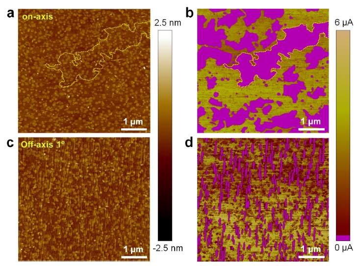
Figure 1. (a, c) C-AFM topography of 1.3 ML MoS2 grown on on-axis and off-axis 1º cut sapphire, respectively. (b, d) The simultaneously acquired C-AFM current maps of (a, c), respectively. Non-homogenous and poorly conductive regions in the first single layer of MoS2 are highlighted in pink by current thresholding (~ 0.3 μA). Images are reproduced with permission.[7] Copyright 2021, American Chemical Society.
Thus, the density of poorly conductive regions is reduced by introducing the off-axis 1º cut sapphire (from 49% to 17% in Figure 1b, d). This density can be further reduced to ~6.5% by skipping the pre-epi treatment process of the sapphire wafers (Figure 2a-b). The shapes of the MoS2 regions with lower conductivity are not random, but correspond to the specific underlying sapphire terraces. The regions with lower MoS2 conductivity on off-axis 1º cut sapphire correspond to the terraces that have bunched together.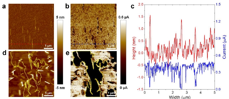
Figure 2. Inhomogeneous electrical conductivity of MoS2 grown on sapphire. (a-b) C-AFM topography and simultaneously obtained current map of 1.3 ML MoS2 on as-received off-axis 1º cut sapphire. (c) Corresponding cross-sectional height (red) and current (blue) profiles at the positions in (a-b), respectively. (d-e) Topography and simultaneously obtained current map of 3.5 ML MoS2 on on-axis cut sapphire. Images are adapted with permission from Ref. [7]. Copyright 2021, American Chemical Society.
During the pre-epi treatment and MOCVD process, steps decompose and agglomerate. Step (de-)formation is primarily driven by the high temperatures used in both pre-epi treatment and MOCVD process. Step bunching becomes more probable as Wterrace narrows, as expected for off-axis 1º cut sapphire. When the monolayer MoS2 is deposited on off-axis 1º cut sapphire without any pre-epi treatment, the density of highly conductive regions increases further from 83% (Figure 1d) to 93.5% (Figure 2b). A clear correlation can be observed between the bunched steps (with a higher Hterrace, 5.8% in Figure 2a) and poorly conductive regions (6.5% dark regions in Figure 2b). The extracted cross-sectional profiles from the topography and current maps in Figure 2c further support this observation. However, the poorly conductive regions are not completely removed in Figure 2b. This should be related to the growth temperature (1000 °C in our work), which is high enough to introduce step bunching on the sapphire surface during the deposition.[8-10]
Regarding the observed inhomogeneity of the MoS2 conductivity distribution, we found that the presence of MoS2 crystals in the non-closed top layers does not influence the conductivity. Indeed, MoS2 regions with lower conductivity remain nearly constant with MoS2 layer thickness, since they also exist in the 3.5 ML MoS2 (Figure 2d-e): A comparison of the dashed yellow outlined regions in topography and current image shows that MoS2 crystals with a misoriented basal plane in the non-closed top layers do not influence the conductivity in that region. Moreover, it is worth to note that the existence of regions with different conductance not only occurs in the MoS2 epitaxial layer, but also in the MOCVD WS2 layer grown on on sapphire, as shown in Figure 3.
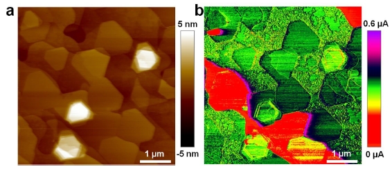
Figure 3. (a-b) Topography and simultaneously obtained current map of 1.7 ML WS2 on on-axis cut sapphire. Images are adapted with permission from Ref. [7]. Copyright 2021, American Chemical Society.
Thus, the lower conductivity relates primarily to the fully closed first MoS2 single layer rather than the nonclosed top layers. Figure 4a-b further supports this by showing two 2nd layer MoS2 crystals with some regions of higher conductivity and some regions of lower conductivity.
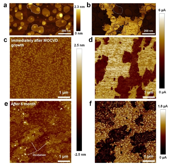
Figure 4. Figure 4. (a-b) Electrical conductivity of 2nd-3rd layer MoS2 islands on the 1.3 ML MoS2 grown on on-axis cut sapphire. (a) Topography and its corresponding (b) current map of the MoS2 grown on on-axis cut sapphire. The white color outlines crystals show partial regions with higher conductivity and partial regions with lower conductivity, indicating that the superficial crystals do not contribute much to the inhomogeneous conductivity of the MoS2 on sapphire. (c-f) Degradation of 1.3 ML MoS2 grown on on-axis cut sapphire. (c-d) Topography and its corresponding current map at 1 V of the 1.3 ML MoS2 collected immediately after the MOCVD growth. (e-f) Topography and current map at 1 V of the same sample after 6 months storage in a N2 cabinet. No oxidized regions in (c), but the MoS2 are partially oxidized in (e), which always correlates to the poorly conductive regions in (f). Images are adapted with permission from Ref. [7]. Copyright 2021, American Chemical Society.
The results indicate that the state of the sapphire starting surface is one of the key parameters determining the physical and electrical properties of the first MoS2 single layer.
Conclusions
The intrinsic electrical properties of 2D TMDs are evaluated via C-AFM and linked to the sample topography. We found a nonhomogenous conductivity in the as-deposited 2D TMDs single layer, which possibly originates from: (i) TMDs surface roughness from TMDs layer thickness variation; (ii) TMDs strain induced by sapphire surface topography; (iii) TMDs intra-grain defectivity due to dependence of TMDs nucleation rate per sapphire terrace; or (iv) TMDs interface defectivity induced by sapphire surface structure and termination, which could result in differently local doping effects. Further investigation is in process to combine C-AFM with advanced spectroscopy techniques (such as Raman, PL and TOFSIMS) to further explore the intrinsic properties of the epitaxial 2D materials.
References
(1) Liu, Y.; Duan, X.; Shin H.-J.; Park, S.; Huang, Y.; Duan, X. Promises and Prospects of Two-Dimensional Transistors. Nature 2021, 591, 43–53.
(2) Su, S.-K.; Chuu, C.-P.; Li, M.-Y.; Cheng, C.-C.; Wong, H.-S. P.; Li, L.-J. Layered Semiconducting 2D Materials for Future Transistor Applications. Small Struct. 2021, 2, 2000103.
(3) Akinwande, D.; Huyghebaert, C.; Wang, C.-H.; Serna, M. I.; Goossens, S.; Li, L.-J.; Wong, H.-S. P.; Koppens, F. H. L. Graphene and Two-Dimensional Materials for Silicon Technology. Nature 2019, 573, 507–518.
(4) Agarwal, T.; Szabo, A.; Bardon, M. G.; Soree, B.; Radu, I.; Raghavan, P.; Luisier, M.; Dehaene, W.; Heyns, M. Benchmarking of Monolithic 3D Integrated MX2 FETs with Si FinFETs. In 2017 IEEE International Electron Devices Meeting (IEDM); 2017; p 5.7.1–5.7.4.
(5) Smets, Q.; Arutchelvan, G.; Jussot, J.; Verreck, D.; Asselberghs, I.; Nalin Mehta, A.; Gaur, A.; Lin, D.; Kazzi, S. E.; Groven, B.; Caymax, M.; Radu, I. Ultra-Scaled MOCVD MoS2 MOSFETs with 42nm Contact Pitch and 250μA/Mm Drain Current. In 2019 IEEE International Electron Devices Meeting (IEDM); 2019; p 23.2.1–23.2.4.
(6) Smets, Q.; Verreck, D.; Shi, Y.; Arutchelvan, G.; Groven, B.; Wu, X.; Sutar, S.; Banerjee, S.; Nalin Mehta, A.; Lin, D.; Asselberghs, I.; Radu, I. Sources of variability in scaled MoS2 FETs. In 2020 IEEE International Electron Devices Meeting (IEDM); 2020; p 3.1.1–3.1.4.
(7) Shi, Y.; Groven, B.; Serron, J.; Wu, X.; Nalin Mehta, A.; Minj, A.; Sergeant, S.; Han, H.; Asselberghs, I.; Lin, D.; Brems, S.; Huyghebaert, C.; Morin, P.; Radu, I.; Caymax, M. Engineering Wafer-Scale Epitaxial Two-Dimensional Materials through Sapphire Template Screening for Advanced High- Performance Nanoelectronics. ACS Nano 2020, DOI: 10.1021/ acsnano.0c07761.
(8) Cuccureddu, F.; Murphy, S.; Shvets, I. V.; Porcu, M.; Zandbergen, H. W.; Sidorov, N. S.; Bozhko, S. I. Surface Morphology of C-Plane Sapphire (α-Alumina) Produced by High Temperature Anneal. Surf. Sci. 2010, 604, 12941299.
(9) Curiotto, S.; Chatain, D. Surface Morphology and Composition of C-, a- and m-Sapphire Surfaces in O2 and H2 Environments. Surf. Sci. 2009, 603, 2688–2697.
(10) Ribič, P. R.; Bratina, G. Behavior of the (0001) Surface of Sapphire upon High-Temperature Annealing. Surf. Sci. 2007, 601, 44–49.