


Making the connection. Atomic force microscopy correlates Graphene’s functional properties on the nanoscale
Ilka M. Hermes,1 Simonas Krotkus,2 Ben Conran,3 Clifford McAleese,3 Xiaochen Wang,3 Oliver Whear,3 Michael Heuken2
1 Park Systems Europe GmbH, Mannheim, Germany
2 AIXTRON SE, Herzogenrath, Germany
3 AIXTRON Ltd, Cambridge, United Kingdom
Introduction
The implementation of graphene in devices for nanoelectronics or energy conversion often requires material modifications e.g., via covalent binding or adsorption. However, the local surface inhomogeneities of pristine graphene such as wrinkles can affect the uniformity of these modifications. Therefore, accurate nanoscale characterization of the graphene topography in combination with the material’s functional properties is essential. Atomic force microscopy (AFM) unites real-space topography imaging with the detection of functional surface properties, including the electronic potential, adhesion, and modulus, and thus offers a holistic approach to the nanoscale characterization of graphene and other 2D materials.
When materials are reduced to two dimensions, unique properties emerge. As such, graphene displays a variety of exceptional physical characteristics, including astonishing charge carrier dynamics, high thermal conductivity, and mechanical strength. Future applications of 2D materials and in particular graphene range from flexible electronics to optoelectronics and electrochemical energy storage. Moreover, the low dimensionality and light weight of 2D materials have attracted the attention of nanoelectronics researchers due to the continuous downscaling of electronic devices.1
Since an industrial application of graphene in electronic devices requires large wafer-scale graphene films, researchers have focused their efforts on improving monolayer growth procedures, with chemical vapor deposition (CVD) on catalytic copper (Cu) as the most explored route. However, graphene growth on Cu substrates entails a subsequent transfer onto an insulating substrate, which can damage the monolayer and introduce contaminations. Therefore, a process for direct growth on insulating substrates is an important step towards future graphene applications.2 In this study, the wafer-scale graphene was grown on LED grade c-plane sapphire in an AIXTRON CCS R&D reactor.
To investigate the morphology and functional properties of CVDgrown graphene on insulating sapphire, AFM with its unique versatility is ideally suitable. Therefore, we have characterized graphene on sapphire with sideband Kelvin Probe Force Microscopy (KPFM) on a Park Systems NX20 AFM. We were able to observe a distinct contrast in the surface potential between graphene and underlying sapphire surface as well as observing variations of surface potential over graphene wrinkles and step edges. The correlation of topographic features and the KPFM surface potential becomes apparent in Figure 1 – a 3D overlay of topography and surface potential. This overlay shows a considerably lower surface potential on graphene wrinkles and around sapphire steps than on the sapphire terraces. Furthermore, the surface potential distribution corresponds to mechanical features, resolved via Park’s PinPoint nanomechanical mode. The correlation of the KPFM and the nanomechanical signals indicates a possible connection between the graphene’s mechanical and electronic properties, thereby demonstrating the potential of AFM as a holistic characterization technique for 2D materials.
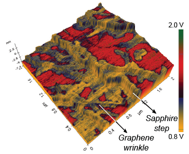
Figure 1. 3D overlay of the graphene topography, which displayed wrinkles and
underlying sapphire steps as indicated, with the surface potential imaged via sideband KPFM.
Surface potential imaging via sideband KPFM
KPFM, an AFM technique, captures the surface topography simultaneously to the surface potential. As a conductive cantilever and conductive or semiconductive sample are electrically connected, their Fermi levels align and a contact potential difference (CPD) arises corresponding to the materials’ work functions. This CPD between tip and sample introduces an additional electrostatic force. In KPFM, the conductive cantilever scans the surface, while applying an AC voltage to detect local changes in this electrostatic force caused by local variations of the CPD according to the surface potential distribution.3 To measure the surface potential locally, a DC bias counteracts the CPD at each point of the scan. Based on the applied DC bias, the surface potential distribution of the sample is reconstructed in the KPFM signal. For the resolution and accuracy of the surface potential in KPFM, the detection method of the electrostatic force is decisive.
In the widely applied off-resonance KPFM, the AC voltage modulates the electrostatic force at a frequency far from the resonance of the cantilever, used for topography imaging. The schematic frequency spectrum of cantilever oscillations in Figure 2a visualizes the separation of the electrical and mechanical excitation at frequencies fAC and f0, respectively. The electrostatic force is detected via the oscillation amplitude at the AC frequency.
By applying a DC bias that matches the potential difference between tip and sample the amplitude at the AC frequency and therefore the electrostatic force is nullified. However, the dependence of the KPFM signal on the long-ranged force lowers the sensitivity of the measurement: non-local interactions between sample and cantilever superimpose on the local signal, which in turn impairs the spatial resolution and accuracy of the surface potential measured via off-resonance KPFM.3
To improve the resolution and accuracy of the KPFM signal, Park Systems has implemented an easy-to-use sideband KPFM mode in their NX research AFMs. In sideband KPFM, a low-frequency AC voltage (2-5 kHz) is applied to the tip to modulate the electrostatic force gradient. The modulated force gradient introduces frequency sidebands on the left and right of the cantilever resonance as shown in the schematic cantilever frequency spectrum in Figure 2b. Analogous to off-resonance KPFM, the feedback of sideband KPFM nullifies the amplitude of these sidebands by applying a DC bias matching the potential difference at each measurement position. By detecting the short-range force gradient instead of the force, long-range crosstalk decreases and the lateral resolution and local potential sensitivity improve significantly.3
By measuring sideband KPFM on the CVD-grown graphene film on a sapphire substrate, we resolved a distinct potential contrast that directly correlates with the topography of the sample (Figure 3). The topography signal showed underlying sapphire terraces and varying step heights of up to 3 nm as well as graphene wrinkles with heights ranging between 0.5 and 2 nm. Interestingly, each sapphire terrace featured finer substructures with elevations of 0.6 nm in proximity to the step edges, visible in the enlarged image detail in Figure 3.
The simultaneously recorded surface potential displayed a clear contrast between two discrete states: we observed a low potential state at the position of the elevations close to the sapphire steps as well as on the graphene wrinkles, and a high potential state on the bulk film on underlying sapphire terraces. For the wrinkle captured in the line profile of Figure 3, we detected a potential contrast of around 0.5 V with respect to the bulk film on sapphire terraces.4 The potential on the elevations close to the sapphire steps, on the other hand, differed by around 0.7 V from the potential of the bulk film on the terraces.
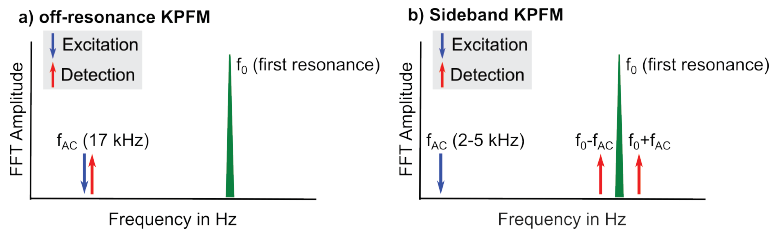
Figure 2. Schematic frequency spectra of the cantilever oscillation for off-resonance KPFM in
a) and sideband KPFM in b).
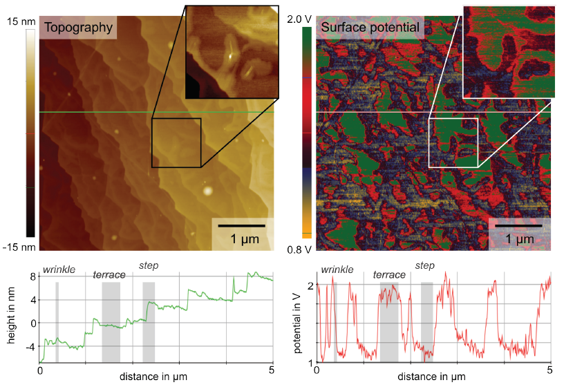
Figure 3. Topography and surface potential captured via sideband KPFM on CVD-grown graphene on a sapphire substrate. The line profiles of the topography in green and the surface potential in red show a correlation of the two signals with a distinct potential contrast between underlying sapphire steps and
terraces as well as graphene wrinkles.
Correlation of surface potential and nanomechanics
To further investigate the graphene wrinkles and the elevations around the sapphire steps as well as their surface potential contrast, we imaged the sample’s adhesion force and modulus in the same position using Park System’s PinPoint nanomechanical mode. PinPoint provides accurate and quantitative nanomechanical images via fast force spectroscopy mapping as shown in Figure 4: the cantilever approaches and retracts at each pixel of the entire scan area to simultaneously acquire 3D topography and nanomechanical information of the sample surface. At each pixel, the XY scanner stops and high-speed force-distance curves are acquired with well-defined control of contact force and contact time between the tip and the sample. The automated analysis of each force curve allows for realtime visualization of sample deformation, modulus, and adhesion force simultaneously to the topography imaging.
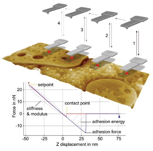
Figure 4. Schematic diagram of Park Systems’ PinPoint nanomechanical mode. In this force spectroscopy technique, the tip approaches the sample and retracts at each pixel before moving to the next pixel, as indicated by positions 1, 2, 3, and 4. The resulting force curves and their automated analysis allow real-time visualization of nanomechanical properties including adhesion force, modulus, stiffness, and deformation.
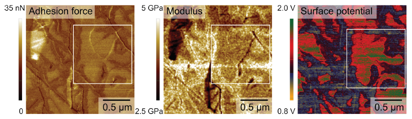
Figure 5. Adhesion force and modulus acquired on graphene on a sapphire substrate via Park Systems’ PinPoint nanomechanical mode and the corresponding surface potential imaged via sideband KPFM at the same measurement area. The white box highlights the same sapphire terrace featuring a higher adhesion force, deformation, and surface potential compared to surrounding sapphire steps.
The adhesion force and modulus acquired via PinPoint nanomechanical mode show a contrast between the underlying sapphire terraces and the steps and graphene wrinkles (Figure 5). As such, the elevations in proximity to the sapphire steps, which also featured a decreased surface potential, exhibit a lower adhesion force and a higher modulus. The lower adhesion and higher modulus suggest that the graphene film becomes harder at these positions. On the sapphire terraces, on the other hand, the adhesion force increases and the modulus decreases. The correlation of the nanomechanical properties with the surface potential and the sample topography indicates a possible connection of the material’s mechanical and electronic properties.
Summary
The combination of different AFM techniques including sideband KPFM and PinPoint nanomechanical mode available on Park Systems’ research AFMs allows a holistic and in-depth characterization of 2D materials as demonstrated on a wafer-scale CVD-grown graphene on sapphire produced in an AIXTRON CCS R&D reactor. The measurements showed a distinct correlation of the sample’s surface potential with the adhesion force and modulus indicating a connection of graphene’s electronic and mechanical properties. Characterizing the highly localized mechanical and electronic properties of 2D materials enables a tailored development for future nanoelectronics applications.
References
[1] S. J. Kim, K. Choi, B. Lee, Y. Kim and B. H. Hong, Annu. Rev. Mater. Res., 2015, 45, 63–84.
[2] N. Mishra, S. Forti, F. Fabbri, L. Martini, C. McAleese, B. R. Conran, P. R. Whelan, A. Shivayogimath, B. S. Jessen and L. Buß, Small, 2019, 15, 1904906.
[3] U. Zerweck, C. Loppacher, T. Otto, S. Grafström and L. M. Eng, Phys. Rev. B, 2005, 71, 125424.
[4] S. Samaddar, J. Coraux, S. C. Martin, B. Grévin, H. Courtois and C. B. Winkelmann, Nanoscale, 2016, 8, 15162–15166.