


Defect Recognition on Coating Layer using PinPoint Nanomechanical Mode, Atomic Force Microscopy
Moses Lee, Jake Kim and Cathy Lee Park Systems Corporation, Suwon, Korea
Introduction
Surface treatment is a critical component in a variety of fields and industries such as automobile1, aerospace2, construction materials3, and mobile and precision4. Surface coating treatment techniques normally involve a coating process, which is widely used industrially to prevent surface abrasion and corrosion. More recently, the ability to convey special properties to coating materials such as anti-static5, antibacterial6 and electromagnetic wave shielding7 have been developed. The popularity of digital devices increased significantly during the 1990’s; this popularity led to rapid developments in industrial coating technologies. These technologies advanced device protection in a number of ways, including scratch resistance, anti-fingerprint, chemical resistance and UV protection.8 Atomic Force Microscopy (AFM), largely used in the field of material surface research, is also utilized extensively on coated surfaces9. From analysis of AFM images, the thickness of the coating can be derived from the morphology of the sample surface while surface roughness yields information about the uniformity of a coating once applied. AFM images allow for a review and inspection of quality control for possible defects. AFM measures both surface morphology and mechanical properties. Using force-distance curves on the coated surface, mechanical properties such as stiffness, adhesion and modulus can be measured10. This application note introduces the latest method developed by Park Systems called “PinPointTM nanomechanical mode” that probes the mechanical properties of a surface. Furthermore, this note describes how the method can be used to analyze the stages at which defects are generated during the material surface processing, specifically during the coating process. In general, defects on the sample surface can be observed through AFM images. However, it is difficult to determine when the defect was generated (during production) solely from surface morphology observation. PinPoint nanomechanical mode resolves this issue: it gathers mechanical information about the coated surface and determines whether defects were created before or after the coating during production.
Materials and Methods
PinPoint Nanomechanical Mode
PinPoint nanomechanical mode collects high resolution topographical data while simultaneously obtaining force-distance data for each pixel of the scan area11. This allows measurement of the sample surface morphology while simultaneously obtaining quantitative nanomechanical properties including modulus, adhesion, deformation, stiffness and energy dissipation.
Experimental Setup
In order to measure mechanical properties of the sample, the PinPoint nanomechanical mode was employed on Park NX10 AFM from Park Systems coupled with an NSC36 cantilever, acquired from MikroMasch. The resonant frequency (f = 130 kHz) and spring constant (k = 2 N/m) of the cantilever allow adequate sample deformation while maintaining sufficient cantilever deflection. The results were analyzed using the Park XEI data processing software, which provides quantitative data from the images, comparisons of mechanical property values, and characterization of the surface material.
Testing Samples
Samples were prepared in two ways to test the ability of the PinPoint nanomechanical mode in distinguishing defects generated before and after the coating application. The first test involved a scratch produced over the surface of a coated glass substrate. The second test featured a scratched glass substrate whose surface was subsequently re-coated. The difference between the creation times of the defect can be determined from whether the glass material was exposed to the scratch site. If the scratch was created prior to coating, the glass will not be exposed, as the coating is applied over the scratch. If the scratched was created after coating, the coating will peel off and expose the glass material. By imaging the site using PinPoint nanomechanical mode, surface mechanical properties (such as adhesion and modulus) show a clear contrast when the AFM tip probes different materials (glass and coating). This information cannot be determined from the topography alone, and Figure 1 clearly shows this.
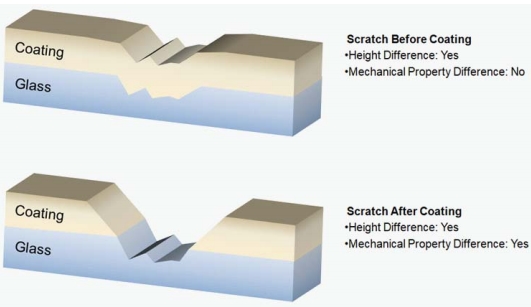
Fig. 1. Illustration of a defect created before and after coating.
The difference between the materials cannot be seen through
the depth of the scratch alone but through the mechanical properties of the material.
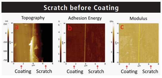
Fig. 2. PinPoint nanomechanical mode images of a glass substrate when the scratch was
created before coating was applied. No contrast was observed between the coated area and the scratched area,
in both adhesion energy and modulus images.roperties of the material.
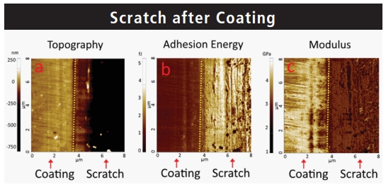
Fig. 3. PinPoint nanomechanical mode images of a glass substrate when the scratch was created
after a coating was applied. The contrast between the coating area and the scratched area is
clearly visible in both adhesion energy and modulus images.
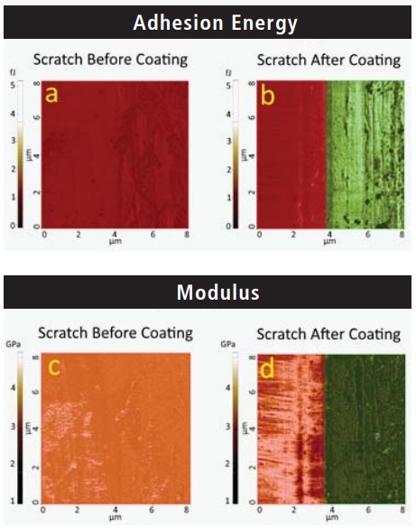
Fig. 4. Region selection applied in Park XEI software,
to calculate mean adhesion and modulus values of each distinct area.
Results
Topography, adhesion energy and modulus images from two samples with defects created before and after coating were obtained using PinPoint nanomechanical mode. The topography images in both cases confirmed the scratch behind a trench (Figure 2a and 3a). Images from this site highlight the mechanical property differences between the scratch area and the unaffected area.
Examining the adhesion energy and modulus images of the scratch before coating (Figure 2b and 2c), they show no visible difference in the mechanical properties between the areas of the scratch and the coating. Figures 3b and c, where the glass substrate is scratched after the coating, show a very clear contrast between the scratch and the adjacent surface. Comparing the mean adhesion energy and modulus values of the surfaces before and after scratching clearly differentiates the two different surfaces. Using Park XEI data processing software, different regions of the same image can be selected i.e. area of the scratch and area of the coating (Figure 4.). For each region, the mean value of each mechanical property was calculated; those values are listed in Table 1 for comparison.
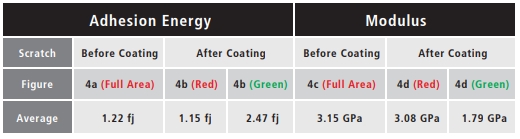
Figure 4a shows the selected coating area which produced a Results 2 Park Systems | Enabling Nanoscale Advances Fig. 1. Illustration of a defect created before and after coating. The difference between the materials cannot be seen through the depth of the scratch alone but through the mechanical properties of the material. Fig. 4. Region selection applied in Park XEI software, to calculate mean adhesion and modulus values of each distinct area. Fig. 2. PinPoint nanomechanical mode images of a glass substrate when the scratch was created before coating was applied. No contrast was observed between the coated area and the scratched area, in both adhesion energy and modulus images.roperties of the material. Fig. 3. PinPoint nanomechanical mode images of a glass substrate when the scratch was created after a coating was applied. The contrast between the coating area and the scratched area is clearly visible in both adhesion energy and modulus images. scratch site. If the scratch was created prior to coating, the glass will not be exposed, as the coating is applied over the scratch. If the scratched was created after coating, the coating will peel off and expose the glass material. By imaging the site using PinPoint nanomechanical mode, surface mechanical properties (such as adhesion and modulus) show a clear contrast when the AFM tip probes different materials (glass and coating). This information cannot be determined from the topography alone, and Figure 1 clearly shows this. Scratch before Coating Scratch after Coating Adhesion Energy Modulus Adhesion Energy Scratch Before Coating 4a (Full Area) 1.22 fj 1.15 fj 2.47 fj 4b (Red) 4b (Green) After Coating Before Coating 4c (Full Area) 3.15 GPa 3.08 GPa 1.79 GPa 4d (Red) 4d (Green) After Coating Figure Average Modulus calculated mean value of 1.22fJ. In figure 4b., the area of the coating and exposed material underneath was selected separately. The adhesion energy value of the coating (1.15 fJ) coincided with the previous value while the adhesion energy of underlying glass substrate exhibited a higher value (2.47 fJ). Also, when comparing the modulus values, the coating from figure 4c gave a calculated value of 3.15 GPa, similar to the modulus value of the coating from figure 4d. (3.08 GPa).
Conversely to the adhesion energy values, the modulus of the scratched glass substrate underneath showed a lower value of 1.79 GPa.
Conclusion
This application note highlights the utility of PinPoint nanomechanical mode from Park Systems to study the mechanical properties of defects to determine whether a surface defect was created before or after the coating process was applied. By measuring the adhesion energy and modulus differences between glass and coating materials, the initial time of the defect formation was successfully identified. AFM can be used for diverse range of applications in the coating industry because of its ability to closely examine the surface properties of samples, properties otherwise not observable by studying morphology alone. By using the PinPoint nanomechanical mode, one can investigate mechanical properties at nanoscale, and study the differences between different coating materials and coating methods. Such benefits will elevate the utility of AFM as a valuable instrument in the coating industry.
References
1. 1. Akafuah, N. K., Poozesh, S., Salaimeh, A., Patrick, G., Lawler, K., & Saito, K. (2016). Evolution of the automotive body coating process—A review. Coatings, 6(2), 24.
2. Benavides, S. (Ed.). (2009). Corrosion control in the aerospace industry. Elsevier.
3. Lee, J., Mahendra, S., & Alvarez, P. J. (2010). Nanomaterials in the construction industry: a review of their applications and environmental health and safety considerations. ACS nano, 4(7), 3580-3590.
4. Leopold, J., Neugebauer, R., Löffler, M., Schwenck, M., &Hänle, P. (2006). Influence of coating-substrate systems on chip and burr formation in precision manufacturing. Proceedings of the Institution of Mechanical Engineers, Part B: Journal of Engineering Manufacture, 220(4), 499-506.
5. Qiu, C., Wang, J., Mao, S., Guo, W., Cheng, S., & Wang, Y. (2010). Preparation of poly (3, 4‐ethylenedioxythiophene)/poly (styrene sulfonate)(PEDT/PSS) composite and its applications in anti‐static coating. Polymers for Advanced Technologies, 21(9), 651-655.
6. Ciacotich, N., Din, R. U., Sloth, J. J., Møller, P., & Gram, L. (2018). An electroplated copper–silver alloy as antibacterial coating on stainless steel. Surface and Coatings Technology, 345, 96-104.
7. Kim, C. G., Nam, Y. W., & Choi, J. H. (2018). U.S. Patent Application No. 15/809,345.\
8. Future Markets. “Automotive.” Nanocoatings. Nov. 2013.
9. Carpick, R. W., & Salmeron, M. (1997). Scratching the surface: fundamental investigations of tribology with atomic force microscopy. Chemical reviews, 97(4), 1163-1194.
10. Butt, H. J., Cappella, B., &Kappl, M. (2005). Force measurements with the atomic force microscope: Technique, interpretation and applications. Surface science reports, 59(1-6), 1-152.
11. John Paul Pineda, Gerald Pascual, Byong Kim, and Keibock Lee (2017). Using AFM PinPointTM Nanomechanical Mode for Quantification of Elastic Modulus in Materials Two Orders of Magnitude Faster than Force Volume Spectroscopy, Park Systems Application note #26