


Tuesday, August 25, 2020
- 01:30 pm-02:30 pm
(SGT)
Singapore - 01:30 pm-02:30 pm
(CST)
Beijing, China - 2:30 pm – 3:30 pm
(KST)
Seoul, South Korea - 2:30 pm – 3:30 pm
(JST)
Tokyo, Japan
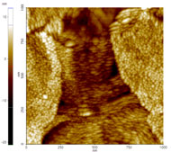
Indium tin oxide (ITO) surface by Non-contact mode, AFM.
The Scanning Probe Microscope (SPM) is not only at the top of the list of equipment pioneering the nano-scale world, it is also the most fundamental technology. Succeeding the first generation optical microscope, and the second generation electron microscope, the SPM has every right to be known as a “third generation” microscopy since it enables us to look into the nano-scale world. At the same time, it has many advantages over manual microscopy which passively look at the samples.
The SPM originated with the invention of the Scanning Tunneling microscope (STM). The STM uses a tunneling current between a probe tip and a sample in a vacuum state to measure surface topography. As a result, it is limited in that it can only measure a sample which is a conductor or a semiconductor. Once the Atomic Force Microscope (AFM) was developed, however, a whole new range of measurement capabilities became possible. Now it is not only possible to measure non-conductors in air, but also to measure the physical, chemical, mechanical, electrical, and magnetic properties of a sample’s surface, and even measure live cells in solution.
The SPM is indeed the key to entering the world of nano-technology that has yet to flourish, and it is essential equipment for various researches in the basic sciences – physics, chemistry, and biology - and in applied industry - mechanical and electrical engineering.
Presented By :
Jake Kim, Park Systems
Dr. Kim received Ph.D. degree in Materials Science and Engineering from Nanyang Technological University, Singapore. He joined Tokyo Institute of Technology International Research Opportunities Program (TiROP) in 2014 and was engaged in nano-scale chemical composition analysis using scanning probe microscopy (SPM). From December 2017, he started to work in Park Systems as the manager of application technology center. He is specialized in the enhancement of nano-machanical measurement performance for Atomic Force Microscopy (AFM), building up a accurate and reliable environment for electrochemical measurement using Scanning Probe Microscopy (SPM; SECM,SECCM) and Scanning Ion Conductance Microscopy (SICM) applications development for biology.