


JAMES HEDRICK
GRADUATE STUDENT, MIRKIN LAB, DEPARTMENT OF CHEMICAL AND BIOLOGICAL ENGINEERING NORTHWESTERN UNIVERSITY
James Hedrick received a S.B., in chemical engineering with a minor in biology from the Massachusetts Institute of Technology. His research work is currently focused on the area of nanolithography. He is developing a method for synthesizing nanomaterial libraries over macro length scales on a single chip. After forming these nanocombinatorial libraries, they can be screened for a multitude of properties for a range of potential applications. Concurrently, he has been researching and building a scanning probe-based 3D printer to print multifunctional materials with nanoscale re solution. He is the owner and founder of his company Pintastic Pins since 2007.
Abstract: Hard Transparent Arrays for Polymer Pen Lithography
Patterning nanoscale features across macroscopic areas is challenging due to the vast range of length scales that must be addressed. With polymer pen lithography, arrays of thousands of elastomeric pyramidal pens can be used to write features across centimeterscales, but deformation of the soft pens limits resolution and minimum feature pitch, especially with polymeric inks. Here, we show that by coating polymer pen arrays with a ~175 nm silica layer, the resulting hard transparent arrays exhibit a force-independent contact area that improves their patterning capability byreducing the minimum feature size (~40 nm), minimum feature pitch (~200 nm for polymers), and pen to pen variation. With these new arrays, patterns with as many as 5.9 billion features in a 14.5 cm2 area were written using a four hundred thousand pyramid pen array. Furthermore, a new method is demonstrated for patterning macroscopic feature size gradients that vary in feature diameter by a factor of 4. Ultimately, this form of polymer pen lithography allows for patterning with the resolution of dippen nanolithography across centimeter scales using simple and inexpensive pen arrays. The high resolution and density afforded by this technique position it as a broad-based discovery tool for the field of nanocombinatorics.
“A CRITICAL PART OF MY RESEARCH IS BEING ABLE TO PATTERN HARD AND SOFT MATERIALS WITH NANO RESOLUTION USING POLYMER PEN LITHOGRAPHY AND DIPPEN NANOLITHOGRAPHY. BOTH TECHNIQUES ARE POSSIBLE USING THE PARK XE-150. ON A DAILY BASIS, I RELY ON THE PARK XE-150 TO CREATE HIGH-RESOLUTION, LARGE-AREA PATTERNED ARRAYS THAT I CAN THEN USE TO SYNTHESIZE AND SCREEN HIGHLY COMPLEX NANOPARTICLES.”
Summarize the research you are doing and explain briefly how it will impact society. Why is your research important?
As materials go from the macro-to-micro and then to the nanoscale, their properties will vastly change. At the nanoscale, small changes in size and composition of material have dramatic effects on the chemical activity, energy capture, and mechanical properties.
Polymer pen lithography (PPL) utilizes an array with millions of pyramidal pens to deposit single attoliter features on a surface. When combined with scanning probe block copolymer lithography, which utilizes PEO-b-P2VP and a metallic precursor to direct the on-surface and spatially confined synthesis of metal nanoparticles, combinatorial libraries of billions of nanoparticles can be synthesized in unison with variations in both size and composition. This innovative, highthroughput screening platform enables rapid discovery of next generation catalysts that have the potential of drastically impacting multiple industries.
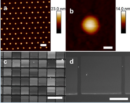
(a) AFM of a dot array with a 190 nm pitch in a hexagonal pattern array written using hard transparent array, 200 nm scale bar; (b) single polymer feature with a circle of small droplets from original meniscus, 20 nm scale bar; (c) dark-field optical microscopy of array with 500 nm pitch written using hard transparent array with PPL with 14 641 features written per pen, 100 μm scale bar; and (d) zoomed in image pattern made form a single pyramidal pen, 25 μm scale bar
Published in: James L. Hedrick; Keith A. Brown; Edward J. Kluender; Maria D. Cabezas; Peng-Cheng Chen; Chad A. Mirkin; ACS Nano 2016, 10, 3144-3148.
DOI: 10.1021/acsnano.6b00528
Copyright © 2016 American Chemical Society