


Technical note for NX-Mask (Novel approach for photomask repair by using AFM)
Application Technology Center
Introduction
The photomask is a key component in photolithography for nano-patterning wafers in semiconductor device manufacturing. A photomask selectively transmits or reflects light to produce a pattern in the target substrate. A defect on the photomask can be caused by absorber patterning or added during mask handling and may deteriorate the quality of the wafer and cause functional flaws in the actual device. To remove these defects, various repair methods are traditionally used including E-beam, ion, laser, and nanomachining. Atomic force microscopy (AFM) images surfaces using a sharp tip of several or tens of nanometers. AFM is widely used in the semiconductor industry as well as the materials, chemical, electrical, electronic, and biological industries. In the semiconductor field the high accuracy and precision of AFM is increasingly crucial for metrology and failure-analysis applications. Here, progressing miniaturization of the process created an increased demand for AFM to fulfill the role of a defect-removal tool. Building on this trend, the same surface non-destructive high-accuracy imaging capabilities of AFM are being applied to photomask repair. In this application, the AFM tip used to image a sample surface is now used to selectively remove defects from a photomask. This process restores the photomask to its original functionality. Park Systems is leading this technological development with the introduction of the NX-Mask automated AFM. This technical note reviews the concept of photomask repair using the Park Systems NX-Mask and provides examples of different use cases.
Park Systems NX-Mask
The NX-Mask is an automated AFM developed for photomask repair (Figure 1). The NX-Mask uses an AFM tip for defect removal with non-destructive sample surface. Because NX-Mask is an automated AFM, the mask repair is capable of removing defects with nanometer-level precision. Also, it can measure the sample surface at the sub-nanometer level, such as measuring the surface roughness and the dimension of patterns, so it can be used in various ways to study the sample other than mask repair.
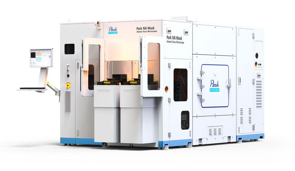
Figure 1. Park Systems NX-Mask
Mask repair process
For photomask repair, the NX-Mask uses a single-crystal diamond tip which enables both highly effective defect removal and tip longevity. The mask repair process consists of 1) survey scan, 2) repair (defect removal), and 3) post-repair imaging (Figure 2). The survey scan determines the exact location and size of the defect of interest with nanometer-level accuracy. After identifying the defect’s location, the NX-Mask removes the defect using the AFM tip. Finally, the post-repair image verifies the effectiveness of the defect removal step. Through the AFM results, each process can be checked in real-time, and the removal of defects can be confirmed by comparing the survey scan with the post-repair imaging.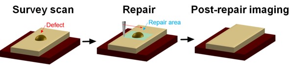
Figure 2. Photomask repair process on the NX-Mask.
Mask repair examples on the Park Systems NX-Mask
In photomask repair on the NX-Mask, there are two categories based on the substrate material and the nature of the defect: 1) soft defect and 2) hard defect. These two categories use the same basic photomask repair sequence outlined above but have slight differences to optimize the results based on the defect type. The first example shown in Figure 3 is the case of a soft defect repair on a photomask pattern. The first image on the left shows the survey scan result with the defect clearly visible in the pattern. After the defect removal step, the post-repair image confirms the successful removal of the defect as shown in the second image on the right. Further, with the non-destructive nature of AFM, it can be confirmed that the photomask pattern is maintained through a comparison of the survey scan and the post-repair imaging, which shows that only defects are selectively removed without any damage to the mask surface.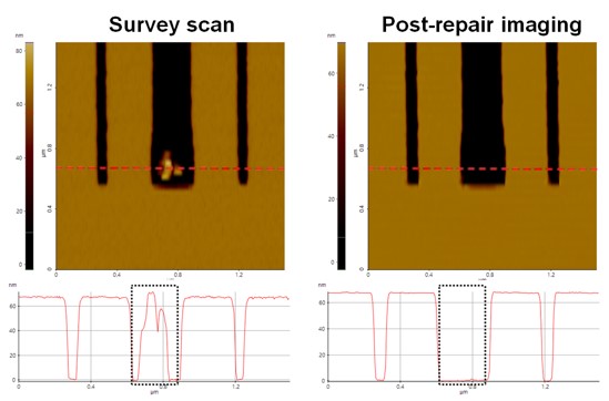
Figure 3. Soft defect repair on photomask.
In another example of soft defect repair, approximately 200 nm tall defect was removed from in the photomask pattern (Figure 4). The defect is identified through the survey scan step and selectively scratched through the repair step. In the repair image of figure 4, it can be seen that a residue of the defect still remains at the bottom of the pattern. However, the partial disintegration makes it easier to remove in an additional repair step, as can be seen in the post-repair imaging in Figure 4. Here, all defects in the pattern were completely removed through the repeated repair process.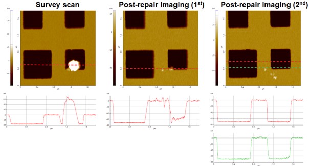
Figure 4. Soft defect repair on photomask. Here, repetitive defect
removal steps were required to eliminate the defect.
Figure 5 shows the result of hard defect repair, i.e., the removal of material within the photomask material itself. The mask repair process follows a similar process as with the soft defect case except in this case the defect is removed by progressively scratching the defect site with the AFM tip while preserving the photomask pattern.
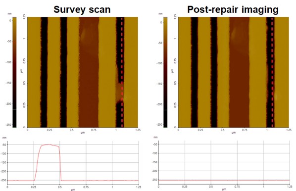
Figure 5. Hard defect mask repair
Conclusion
This technical note demonstrates the mask repair capability of the Park Systems NX-Mask in soft defect and hard defect removal cases. In a stepwise process consisting of Survey scan/ Repair/Post-repair imaging, the defects were accurately identified on the photomask surface and subsequently removed/moved selectively without damage to the photomask surface as confirmed by the final post-repair imaging. The use of AFM in the semiconductor industry goes beyond simply measuring the sample surface and is being used in a variety of ways. The mask repair method by Park Systems NX-Mask points to another versatile application for AFM that can keep pace with the increasingly challenging demands of photolithography in the semiconductor industry.