


Vladimir Korolkov, Ilka M. Hermes
Park Systems UK Ltd, MediCity, Nottingham, UK.
Park Systems Europe GmbH, Mannheim, Germany
After discovery of groundbreaking properties of graphene in 2004,1 possible applications for 2D materials in nanoelectronics, flexible optoelectronics and electrochemical energy storage have been extensively studied.2 To achieve a larger variety of materials properties that can potentially be tailored to each application, researchers investigated Van der Waals heterostructures with different 2D materials stacked on top of each other in a new research field called twistronics.3 They found that, due to the different periodicity of materials and slight twist angle between the two layers, superlattices emerge, which feature a larger periodicity than the pristine monolayers.4
These superlattices are Moiré patterns. Essentially, a Moiré pattern is an interference pattern introduced by overlaying similar but slightly offset periodic structures (Figure 1). For 2D materials, this pattern can either occur in microstamped Van der Waals heterostructures or layers grown via plasma-enhanced chemical vapor deposition (CVD) or molecular beam epitaxy (MBE).4
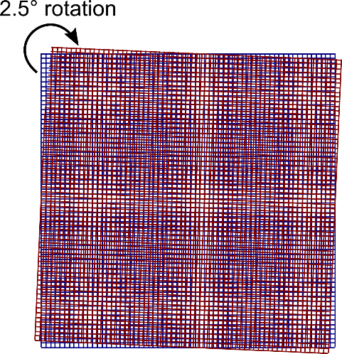
Figure 1: Moiré pattern introduced by superposition and 2.5° twist angle of two periodic structures.
To correlate and tune the periodicity of the Moiré pattern to material properties such as superconductivity, ferromagnetism or conductive topological channel accurate imaging of Moiré patterns is vital for research and future application of Van der Waals heterostructures in industry. Atomic force microscopy (AFM), a real-space, high resolution imaging technique, can not only capture superlattices in the sample topography but also allows the visualization of Moiré patterns in the samples’ electromechanical response.5 Since typical corrugation variations on Moiré patterns are around 10 – 50 pm in height, their visualization requires AFMs with a low noise performance in all major imaging modes. In particular, contact mode imaging of Moiré patterns is a benchmark noise test for any AFM.
Here, we show how Park Systems’ large sample NX20 AFM resolves Moiré patterns with different periodicities ranging from 11 to 15 nm on a graphene/hBN (hexagonal boron nitride) Van der Waals heterostructure.
In this instance, we used a microstamped graphene layer on top of hBN monocrystalline flake. Such sample typically displays both wrinkles and bubbles in the sample topography, as well as many flat areas that exhibit Moiré patterns (Figure 2 and 3).
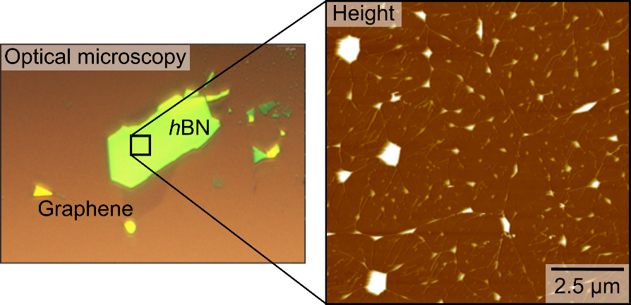
Figure 2: Optical microscopy image of a graphene flake stacked on top of a hBN flake with a large are height image of the graphene topography. Sample courtesy: Dr. Ziwei Wang, The University of Manchester (www.artem-lab.com)
These Moiré patterns have been successfully imaged in both contact and tapping modes. Tapping mode image clearly displays three main features of microstamped graphene: wrinkles, a bubble and areas with different Moiré patterns (I - III). These varying Moiré patterns originate from slight angle mismatches between atomic lattices of graphene and hBN that happens during microstamping.
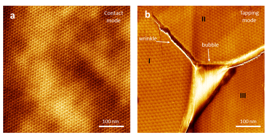
Figure 3: Two different areas of graphene/hBN displaying Moiré patterns. Imaged in contact (a) and tapping modes (b). Moiré pattern periodicities are 11.2 nm (a) and 14.5nm (Ib), 12.4nm (IIb) and 10.9nm (IIIb).
Summary
By resolving Moiré patterns on a graphene/hBN heterostructure in both contact and tapping modes, we have demonstrated the capabilities of the large sample NX20 AFM for high resolution, low noise imaging, required for an accurate characterization of superlattices in stacked 2D materials. Thereby, our results highlight the potential of Park Systems AFMs to advance academic and industrial research in the field of twistronics.
Source
1. Novoselov, K. S. et al. Electric Field Effect in Atomically Thin Carbon Films. Science (80-. ). 306, 666 LP – 669 (2004).
2. Kim, S. J., Choi, K., Lee, B., Kim, Y. & Hong, B. H. Materials for Flexible, Stretchable Electronics: Graphene and 2D Materials. Annu. Rev. Mater. Res. 45, 63–84 (2015).
3. Carr, S. et al. Twistronics: Manipulating the electronic properties of two-dimensional layered structures through their twist angle. Phys. Rev. B 95, 75420 (2017).
4. He, F. et al. Moiré Patterns in 2D Materials: A Review. ACS Nano (2021). doi:10.1021/acsnano.0c10435
5. McGilly, L. J. et al. Visualization of moiré superlattices. Nat. Nanotechnol. 15, 580–584 (2020).