


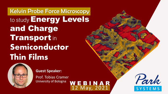
Kelvin Probe Force Microscopy to Study Energy Levels and Charge Transport in Semiconductor Thin Films
Wednesday, 12 May, 2021
- 10:00 am – 11:30 am
(GMT)
London, Dublin - 11:00 am – 12:30 pm
(CET)
Berlin, Paris, Rome - 18:00pm – 19:30 pm
[UTC+9]
Seoul, Tokyo
Abstract:
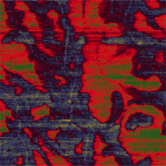
Semiconductor thin films with engineered electrical and mechanical properties are at the very heart of emerging applications in different areas such as flexible electronics, optoelectronics or bioelectronic sensors. Research in material deposition and processing is providing an ever-increasing arsenal of techniques enabling finetuning of basic semiconductor properties. In order to assist these efforts, nanoscale characterization techniques are needed that reveal morphology and provide at the same time access to local electromechanical characterization, providing means to verify efficiency and homogeneity of treatments. In this seminar I will present two examples from our group’s work that illustrate Kelvin-Probe Force Microscopy in the characterization of novel semiconducting thin films. In a first example I will introduce the investigation of molecular surface treatments to shift halide perovskite workfunctions over an interval exceeding 1.0 eV.(1) Such an unprecedented control on energy levels has significant impact on perovskite solar cell and detector research. The second example introduces to the characterization of local transport properties in printed organic semiconducting microcrystals.(2, 3) Here, KPFM enables to resolve the evolution of nanoscale fracture lines caused by surface strain during bending. With KPFM one can characterize the barrier height for transport across such fractures and rationalize their impact on device deterioration in flexible electronics applications.
1. L. Canil et al., Tuning halide perovskite energy levels. Energy Environ. Sci. (2021), doi:10.1039/d0ee02216k.
2. S. Lai et al., Morphology Influence on the Mechanical Stress Response in Bendable Organic Field-Effect Transistors with Solution-Processed Semiconductors. Adv. Electron. Mater. 1700271, 1–9 (2017).
3. T. Cramer et al., Direct imaging of defect formation in strained organic flexible electronics by Scanning Kelvin Probe Microscopy. Sci. Rep. 6, 38203 (2016).
The theoretical introduction to KPFM will be presented by Ilka Hermes, the Principle Scientist at Park Systems Europe
Presented By :
Ass. Prof. Tobias Cramer, Department of Physics and Astronomy, University of Bologna, Viale Berti Pichat 6/2, Italy
tobias.cramer@unibo.it
Tobias studied chemistry and physics at the University of Freiburg (D) and finished in 2006 with a Ph.D. degree. After a period of post-doctoral fellowships with stays in Germany (Institude for Advanced Studies, Freiburg), Italy (Faculty of Chemistry and Institute for the Study of Nanostructured Materials – ISMN-CNR, both Bologna) and United States (The Scribbs Research Institute, San Diego), he is now working as an Associate Professor in the Faculty of Physics at UNIBO. Tobias is interested in flexible electronic sensors and transducers with applications in Human-Technology Interfaces, Life-Sciences and radiation sensing. The leitmotiv in his research is charge transport phenomena in condensed matter, which Tobias has investigated by theoretical and experimental methods. Tobias is co-author of +55 scientific articles and book chapters, his h-index is 21.