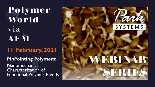
Thursday, 11 February, 2021
- 10:00 am – 11:30 am
(GMT)
London, Dublin - 11:00 am – 12:30 pm
(CEST)
Berlin, Paris, Rome - 18:00pm – 19:30 pm
[UTC+9]
Seoul - 18:00pm – 19:30 pm
[UTC+9]
Tokyo

Polymer based blends and composites are a key area of materials research activity. For example,
blends of polymers are used in optoelectronic devices for charge extraction, and biopolymers
which change their mechanical character upon environmental influences. Like bio-molecules, a
hierarchy of structure exist in synthetic polymers as well. Synthetic polymers allow control of
bulk properties from bottom upwards in hierarchical manner. For example, composition of the
macromolecular chain, chain conformation in an ensemble, and its blend/composite with other
materials are all parameters for enhancing their performance. Tuning of bulk properties by
adjusting structure at these widely varying scales is at the core of study and development of
polymers. Therefore, visualizing structure at nanometers to hundreds of micrometers provides
insight for both fundamental and applied research. Moreover, for functional polymers correlating
their electrical, piezoelectrical, and nanomechanical properties with macromolecular structure
is a significant task. Atomic force microscopy-based techniques are ideal for investigations of
functional characteristics simultaneously with structure in a wide range of environmental
conditions.
In this webinar, we will describe and demonstrate polymer characterization using PinPointTM
mapping on Park System’s NX10 atomic force microscope. Additionally, we will demonstrate example
measurements where electrical property maps are acquired simultaneously with topography and
nanomechanical maps.
[1] Vancso, G. and Schönherr, H., “Scanning Force Microscopy Of Polymers” 1st ed.
Springer-Verlag Berlin Heidelberg.
[2] Hayakawa, T. and Horuchi, S. “From Angstrom to Micrometers: Self-Organized Hierachical
Structure within a Polymer Film” Angewandte Chemie, 42, (2003)

Presented By :
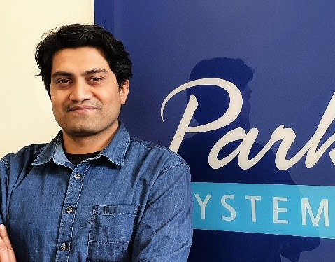
Abdul Rauf, Application Scientist at Park Systems
Europe
Abdul is an Application Scientist at Park Systems Europe, where he supports development of AFM solutions for customers. He had his training as a polymer materials’ engineer with emphasis on elastomer blends and composites. Abdul has expertise in characterization of macromolecular systems at interfaces. He worked on his doctoral thesis in the group of Prof. Jürgen P. Rabe in Humboldt-Universität zu Berlin, where he acquired expertise in morphological and nanomechanical characterization of thin films confined in interfaces. His work in Berlin also included study of two-dimensional materials such as monolayers of Graphene, Hexagonal Boron Nitride, and Transition Metal Dichalcogenides as sensors for strain transfer across atomic interfaces.


