


Akshay Gowda, a graduate student working with Dr. S.V.BABU, distinguished university professor, Clarkson university receives the PARK AFM scholarship award
Title of Research Paper:
Post-CMP Cleaning of Ceria Particles from Silicon Dioxide and Nitride Wafers for Advanced Technology Nodes
Abstract:
Advanced device manufacturing requires stringent process conditions to prevent defects that can lead to device failure and reliability issues. In particular, defects such as residual particles, foreign materials, scratches, etc. should be removed from the wafer surface aft er chemical mechanical planarization (CMP).
How do you use AFM in your research?
Chemical mechanical planarization (CMP) is one of the most crucial steps in the manufacturing of integrated circuits (ICs). In a typical CMP process, a wafer is pressed against the polishing pad fixed to a rotating platen and the chemical slurry (consisting of abrasive particles and necessary chemical additives) is supplied on to the pad. The wafer is polished by the combination of chemical and mechanical forces. CMP inevitably introduces surface defects and contaminants due to the presence of chemical additives and abrasive particles in the slurry used to planarize wafer surfaces. Surface particles are one of the major defects induced by CMP. If not removed, they can cause short or open circuits and affect the final device performance and reliability. Therefore, cleaning such particlulate defects on wafer surfaces post- CMP is critical for successful manufacturing of ICs to improve productivity. Billion or so active transistors in each IC is electrically isolated using shallow trench isolation (STI) CMP. Ceria particle-based slurries are used to polish STI structures. Due to high chemical affinity of ceria particles to silicon dioxide surfaces, STI CMP leads to particle contamination making post-CMP cleaning challenging as ceria particles adhere very strongly to STI wafers during polishing. In our research, we are developing cleaning chemistries than can remove ceria particles from silicon dioxide wafers. The particles on silicon dioxide wafer surfaces before and after cleaning are imaged using atomic force microscopy (AFM) and counted.
Subsequently, cleaning efficiency is calculated to evaluate the effectiveness of the developed cleaning chemistry.
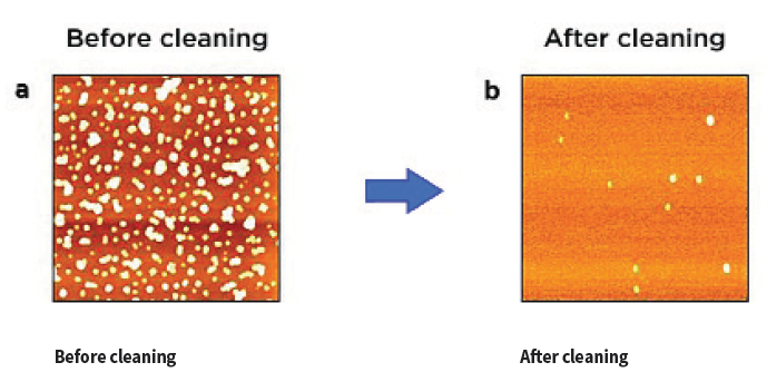
Figure 1. AFM image of silicon dioxide wafer surface (a) contaminated with ~30 nm (mean diameter) ceria particles and (b) cleaned with a cleaning solution In this case, the number of particles before and after cleaning is 290 and 12 respectively and the corresponding cleaning efficiency is 96%.
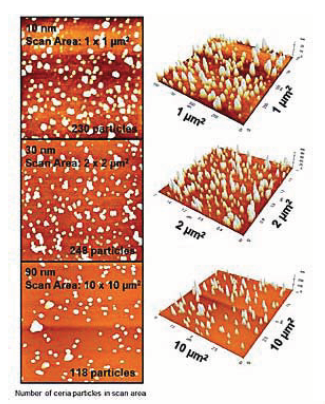
Figure 2. Topographic images of adsorbed ceria particles on silicon dioxide wafer surfaces in scan areas of 1 × 1 μm2 (for ~10 nm ceria particles), 2 × 2 μm2 (for ~30 nm ceria particles) and 10 × 10 μm2 (for ~90 nm ceria particles). Different scan areas were chosen for different sized particles to obtain adequate number of particles in AFM images.
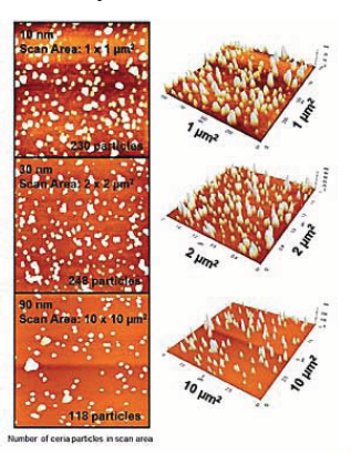
Figure 3. AFM images of adsorbed ceria particles on silicon dioxide wafer surfaces and the corresponding number of particles before and after cleaning with standard clean 1 (SC1) solution in scan areas of 1 × 1 μm2 (10 nm-ceria), 2 × 2 μm2 (30 nm-ceria), and 10 × 10 μm2 (90 nm-ceria).