


Electrical Characterization using Scanning Microwave Impedance Microscopy
Armando Melgarejo1, Nicholas Antoniou2
1 Park Systems, Inc.
2 PrimeNano, Inc.
Introduction
Understanding the electrical properties of materials is a growing concern in materials research and the semiconductor industry. As a result, new and existing technologies are being adapted to address the limitations of currently used methods. This technical note introduces ScanWave Scanning Microwave Impedance Microscopy (sMIM) as a new imaging mode for Park Systems Atomic Force Microscopes (AFM). sMIM uses microwave reflections from the tip-sample nanometric interaction to gather the local electrical properties of a sample, such as permittivity and conductivity. These two properties can then be converted to dielectric constant, capacitance, resistivity and dopant concentration (for semiconductors) at the nanoscale (Figure 1). Knowledge of these properties is important to maintain good quality and reliable processing of materials like semiconductors, thin films, and dielectrics.
- ScanWave offers several crucial advantages over other electrical AFM modes such as:
- sMIM is based on a microwave signal, so little to no sample preparation is needed.
- There is no need for a path to ground through the sample since there is no current flow through the sample.
- Floating insulators/dielectrics can easily be directly imaged.
The response of sMIM to capacitance/dielectric constant and dopant level is log-linear (Figure 2) making quantification easy. Compared to SCM (Scanning Capacitance Microscopy), sMIM provides DC capacitance, DC resistance, and dC/dV and dR/dV. SCM only provides dC/dV and in addition, is much harder to quantify. SSRM (Scanning Spreading Resistance Microscopy) and SCM both require elaborate sample prep and setup. Lastly, ScanWave Pro has a capacitance sensitivity of 0.075 aF which enables the imaging of minuscule variations in capacitance, resistance and dopant levels all the way to intrinsic silicon (see Figure 2). Capacitance vs Voltage (C-V) is a commonly used measurement technique for semiconductors and by sweeping a DC voltage on probe, C-V measurements can be taken with nanoscale positioning.
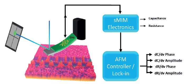
Figure 1. Diagram of the fundamentals of Scanning Microwave Impedance Microscopy (sMIM). The microwave signal is transmitted via the shielded probe to the tip where it will interact with the sample. The reflected waves are collected and transmitted back to the ScanWave electronics where they are demodulated into relative capacitance and resistance. By adding an AC signal on top of the microwaves and using a lock-in amplifier, properties like phase and amplitude for dC/dV or dR/dV can be measured.
Using PrimeNano’s ScanWave sMIM module on Park Systems AFMs, high-quality images of variations in conductivity and permittivity can be obtained [1]. The combination of AFM and sMIM results in the simultaneous measurement of different channels: capacitance variations, resistance variations, dC/dV amplitude and phase, dR/dV amplitude and phase and surface topography (other mechanical information is also available concurrently). In semiconductors, dopant carrier concentration and type are found through a reference sample.
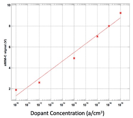
Figure 2. ScanWave Response to Dopant Concentration.
- Furthermore, Park Systems not only offers the combination of non-contact mode imaging which eliminates sample damage but boosts sMIM by combining it with PinPoint [2] and QuickStep [3] technology. These advanced sMIM techniques not only allow high-quality electrical characterization of challenging samples but also exhibit the following advantages:
- Elimination of shearing forces associated with contact-based electrical modes which may otherwise lead to scanning artifacts and sample damage.
- Reduction in tip wear ensures a sharper tip for a longer time.
- Enabling correlative microscopy using multichannel measurements: user can simultaneously obtain not only electrical properties but also nanomechanical properties such as Young’s modulus.
Additionally, PrimeNano offers ScanWave ProTM Solutions [4] which is an automated technique to quantify dopant measurements. It has a dopant spatial resolution of 10 nm and a repeatability of better than 0.1 of a decade of dopant level.
Experimental
sMIM imaging is available with all current Park AFM research systems. SmartScanTM [5] along with Scanwave [1] provide the interface to collect the microwave signals and generate AFM images. Commercially available cantilevers that have a shielded signal path to the tip are needed.
The operational scheme from mounting the tip, creating the near-field electromagnetic wave at the tip, and getting the final image are explained in the following outline. The entire process can be executed in four simple steps:
i. In the first step, tip and sample are mounted and the beam-bounce system is aligned using SmartScan’s guided mode.
ii. Once the tip is ready, the Auto mode on SmartScan will complete step 2 by bringing tip and sample close to each other.
iii. Once tip and sample are in close proximity, ScanWaveTM sends microwaves to the shielded probe to create a localized electromagnetic wave at the apex of the tip. After the electromagnetic near field interacts with the sample, a microwave signal is sent back to the ScanWave electronics for demodulation. All of this is done automatically by the ScanWave software.
iv. The system begins AFM scanning and data acquisition. The user can select the desired scan parameters or let SmartScan choose them.
Result
All images from SRAM sample shown in Figure 3 were acquired simultaneously. Data depicts only a section of two SRAM cells, NMOS transistors shown. Figures 3.b and 3.c are the phase and amplitude of the dC/dV channel respectively. The dC/dV phase (Figure 3.b) reveals that the SRAM sample is mainly composed of N-dopant, pink areas (source/drain regions) and P-dopant for the channel (black regions). While the dC/dV amplitude depicts the variations of the dopant concentration among the sample, white regions/implants are the channel areas that have lower doping than the source/drain areas.
For the reference sample depicted in Figure 4, the goal was to measure capacitance across it. Figure 4.b depicts the changes in capacitance across the sample that correspond to the relative amount of dopant concentration. The reference standard is made of steps of increasing N-type dopant from the left side to the center and decreasing p-type dopant steps from the center to the right edge. Scanning a reference sample allows verification of the technique sensitivity and helps to demodulate the phase signal, allowing the separation and measurement of capacitance and resistance channels. Furthermore, it allows to establish a reference value that enables subsequent quantification of the measured data.
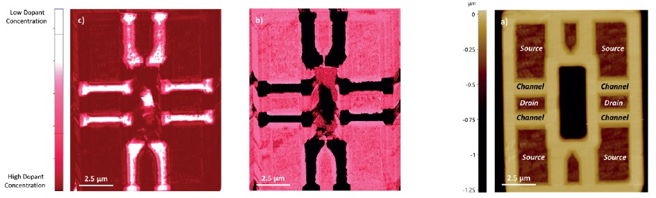
Figure 3. Static Random Access Memory (SRAM). Only N-type metal oxide semiconductor (NMOS) implant is shown in the results (a) Topography Image depicting a subunit of the memory. (b) dc/dv phase image. The contrast corresponds to the dopant type, the selected implant is mainly composed of N-dopant structures, pink areas. (c) dc/dv amplitude image, reveals the dopant concentration. Red areas have a smaller concentration of dopant in comparison to the white regions of the NMOS.
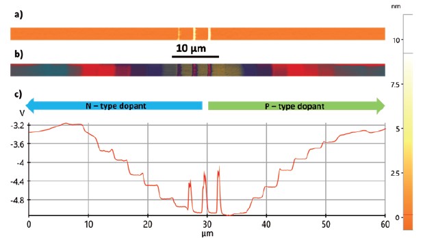
Figure 4. Dopant implant reference sample with a staircase of P and N doped regions. (a) Topography image. (b) Capacitance channel, image resolves variations at the mV scale. (c) Line profile of capacitance information.
Conclusion
This technical note gave an introduction about the capability of Scanning Microwave Impedance Microscopy to obtain high-quality data of electrical properties from diverse samples. ScanWaveTM in combination with Park AFMs is a powerful characterization tool for development and quality control of semiconductor manufacturing steps such as dopant incorporation and dielectric film formation. Additional nanoelectrical characterization for semiconductors, dielectrics, metal oxides, ferroelectrics and 1D and 2D materials are among the potential applications of sMIM.
Reference
[1] ScanWaveTM Primenano: https://primenanoinc.com/index.html
[2] Park Systems Corp. (2022). PinPoint Nanomechanical mode. Suwon, South Korea: https://www.parksystems.com/index.php/park-spm-modes/97-mechanical-properties/3601-pinpoint-nanomechanical-mode
[3] Park Systems Inc (2021). Accurate dopant profiles of semiconductor device structures with QuickStep. California, USA.: https://www.parksystems.com/applications/electrical-electronics/semiconductor/387-accurate-dopant-profiles-of-semiconductor-device -structures-with-quickstep-scanning-capacitance-microscopy?highlight=WyJxdWlja3N0ZXAiLCIncXVpY2tzdGVwJyJd >
[4] ScanWave Pro Solutions. California, USA.: https://primenanoinc.com/new!-scanwave-pro%e2%84%a2-solution.html
[5] Park SmartScan : Park AFM Operating Software https://parksystems.com/products/operating-software/park-smartscan
[6] Proceedings Volume 11611, Metrology, Inspection, and Process Control for Semiconductor Manufacturing XXXV; 116110K (2021): https://doi.org/10.1117/12.2584560.