


Surface potential measurements of 2D materials in high vacuum
J. Serron, A.Minj, L. Wouters, T. Hantschel
IMEC, Leuven, Belgium
Introduction:
With the scaling of conventional field effect transistors (FETs), it becomes increasingly important to overcome adverse short-channel effects. Here, two-dimensional (2D) materials, which confine carriers within one plane, can improve electrostatic gate control and further extend Moore’s Law. Among 2D materials, transition metal dichalcogenides (TMDs) are composed of one layer of transition metals, M, sandwiched between two layers of chalcogen atoms, X, forming the chemical formula MX2. MoS2, WS2, MoSe2 and WSe2, which are common TMDs, possess semiconducting properties due to their crystalline lattice structures. Their monolayers display a direct bandgap and can show outstanding electrical, optical, and mechanical material characteristics. Extensive research on TMDs is currently performed, as tremendous impact is expected in the fields of nanoelectronics, optoelectronics and the manufacturing of novel devices.
Because of the low out-of-plane conductivity and susceptibility to easily tear, the characterization of mono- to few-layer TMDs can be challenging. Only a handful techniques such as Raman, Photoluminescence Spectroscopy and Atomic Force Microscopy (AFM) based techniques can provide required information on structural and electronic properties in a short time span. In addition to the statistical analysis of TMD roughness and layer step heights via AFM, the AFM-based Kelvin probe force microscopy (KPFM) is increasingly used to visualize charging effects in 2D/substrate systems, probe charge transfer in 2D/2D heterostructures and grain boundaries [1, 2, 3].
KPFM allows the characterization of electronic properties of surfaces and devices at the nanoscale. It is primarily used to image surface potential distributions on conductive and semiconductive materials by probing the contact potential difference (VCPD) between an AFM tip and a sample [4]. Thus, this technique can collect information on work functions, material inhomogeneities, local trapped charges, embedded nanostructures, interconnect faults etc. [5, 6]. When a conductive AFM tip is electrically connected to a conductive or semiconducting sample, the Fermi levels of the tip and sample align. Hence, electrons flow from the material with a lower work function to the one with a higher work function until an equilibrium state is reached (i.e., the Fermi-levels are aligned). The redistribution of charges on the two surfaces introduces an electrostatic force between tip and sample, which is proportional to the difference of their work functions. To nullify this electrostatic force an external DC bias is applied between tip and sample; the so-called contact potential difference VCPD [1].
It is defined as:
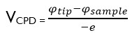
φtip and φsample are the work functions of the tip and the sample, respectively and e is the elementary charge.
Figure 1: Band alignment diagrams of electrically connected tip-sample system with zero DC bias on the left and with DC bias = -VCPD on the right. This schematic is valid only for work functions φSAMPLE ≠ φTIP leading to a non-zero electric field between tip and sample. EF is the energy of the Fermi levels and Evac is the energy of the vacuum level.
As a dynamic AFM method, KPFM can be operated in amplitude modulation or via sideband mode in Park System AFMs. In Park’s sideband KPFM, the VCPD depends on the electrostatic force gradient instead of the long-range electrostatic force, which facilitates a high electrical sensitivity and a spatial resolution, which is mainly limited by the tip radius. Analytical calculations have shown that for a commercial tip geometry a spatial resolution as close as 10nm can be achieved on a planar surface [7]. For a better understanding of the KFPM principle we refer to the application notes “ How to obtain sample potential data for KPFM measurement” by Hosung Seo, Dan Goo and Gordon Jung, Park Systems Corporation as well as “ Surface Potential Imaging via Sideband Kelvin Probe Force Microscopy” by Armando Melgarejo, Ben Schoenek and Byong Kim, Park Systems, Inc.
In order to obtain reliable and quantitative surface potential measurements on TMDs via sideband KPFM, it is crucial to consider the materials’ receptivity to sample surface changes by gas species. In the future, the changes of TMD properties due their surface reactivity could even be exploited for molecule sensing applications. Here, a direct comparison of the surface potential of MoS2 in ambient and high vacuum conditions in Park’s NX-Hivac highlights the impact of gas species on the sample surface and shows the necessity of environmental control for quantitative TMD characterization.
Experimental:
Sideband KPFM allows to measure the surface potential by nullifying the electrostatic force gradient formed between the sample surface and the metallic AFM tip through a fast DC feedback. In our setup in the Park Systems’ NX-Hivac, the sample is grounded and generally an AC bias between 0.5 V to 3.0 V is applied at a frequency in the range of 2.0 – 5.0 kHz to modulate the electrostatic signal. The typical scan rate for KPFM measurements ranges from 0.1 Hz to 0.3 Hz. For this dataset, commercially available Au-coated Si AFM probes with a spring constant of k ~ 5N/m and a natural frequency f0 ~ 150 kHz were used.
Results and Discussion:
In this experiment, the surface potential of a MoS2 flake transferred on SiO2 was investigated via sideband KPFM in air and high vacuum (~10-5 Torr) using a Park NX-Hivac (Figure 2). A striking difference in the surface potential distribution on the flake for both types of environmental conditions was observed.
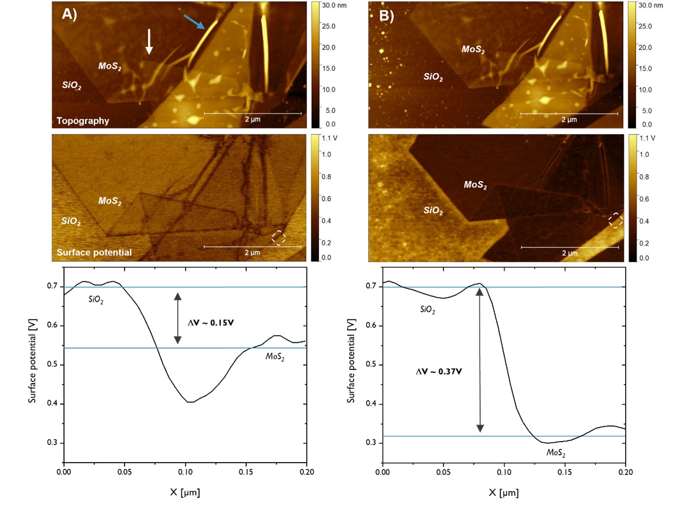
Figure 2: Surface potential maps of a MoS2 flake transferred onto a SiO2 substrate in air (A) and high vacuum (B), with corresponding topography and cross section graphs extracted along the dashed white box.
As shown in the morphology in Figure 2, the MoS2 flake was not transferred uniformly on the SiO2 substrate, but showed folds and wrinkles in some regions, indicated by the white and blue arrow, respectively. When analyzing the surface potential distribution this is important to take into consideration as layer thickness and local strain are known to influence the surface potential in 2D materials. In ambient environment, a surface potential difference of ~0.15 V was observed between the transferred MoS2 flake and the SiO2 substrate (Figure 2A) with a lower magnitude for the latter. When measuring in high vacuum, this difference was significantly enhanced to a value of ~0.4 V (Figure 2B). The small potential difference measured between the MoS2 flake and SiO2 in ambient environment can most likely be attributed to the presence of a surface water layer with thicknesses of up to 2 nm and/or oxygen, which alters the surface potential of the MoS2 flake through charge transfer, and subsequently changes its work function. In addition, it is important to acknowledge that due to the differences in wettability of MoS2 and SiO2 the screening of the actual surface potential by varying water layer thickness can induce an error in KPFM measurements. Under high vacuum conditions, more details and contrast reversals in the surface potential were revealed, since the influence of water and/or oxygen is eliminated. For example, a drop in surface potential at the wrinkles of the MoS2 flake was present in both experimental conditions, but solely in high vacuum its enclosure by a higher potential boundary was revealed. A clear insight on the potential distribution developed at and around wrinkles could provide a better understanding of their impact on device current transport properties. This experiment highlights the impediment in probing intrinsic electronic properties for 2D materials and assessing the true surface potential while measuring in air.
Conclusion:
This Application Note demonstrates the importance of high vacuum environment for reliable and accurate surface potential characterization of 2D materials using KPFM. The surface potential of mono- to few-layered MoS2 under ambient conditions deviates significantly from the values obtained in high vacuum: When moving from ambient to high vacuum environment in Park’s NX-Hivac, the surface potential difference between the MoS2 flake and SiO2 substrate increases from 0.15 V to 0.4 V. The small potential difference observed in ambient conditions is indicative of the presence of a thin surface water layer that screens the true surface potential of the sample. In vacuum conditions, the water molecules desorb over time. Hence, their influence on the electronic properties of the 2D materials drastically decreases, which ensures a more reliable and accurate surface potential measurement.
References:
[1] Datta et al. Nano Letters 9, pp. 7-11 (2008)
[2] Sharma et al. Appl. Phys. Lett. 110, 061602 (2017)
[3] Moore et al. npj 2D Materials and Applications (2020)
[4] M. Nonnenmacher, M. P. O’Boyle, and H. K. Wickramasinghe, Appl. Phys. Lett. 58, 2921 (1991)
[5] C. Barth et al 2010 New J. Phys. 12 093024
[6] S. Sadewasser, T.Glatzel, Kelvin probe force microscopy, Vol. 65, Springer Series in Surface Sciences
[7] J. Colchero, A. Gil and A. M. Baro, Phys. Rev. B, 64, 245403 (2001)