


Armando Melgarejo, Cathy Lee, Charles Kim, Ben Schoenek, Jiali Zhang, Byong Kim,
and Stefan Kaemmer, Park Systems Corporation
Introduction
This technical note introduces Park FX40, the new research grade Atomic Force Microscope (AFM). Wide scale acceptance of AFM was previously hampered by complex operation and handling. FX40 overcomes these hurdles by introducing intelligent scan algorithms, fully automated tip handling, fully automated detection systems alignment and tip approach, and a multi-sample chuck. Building on the cross-talk elimination design of the XE- and NX-series of AFMs, FX40 additionally increases performance and improves productivity that is accessible to everyone. With the FX40, high-definition and meaningful data can be obtained with just a few clicks. Additional built-in environmental sensors open new application spaces that will be discussed in a later publication. This technical note describes the imaging process from beginning to end and illustrates it with real-world application examples.
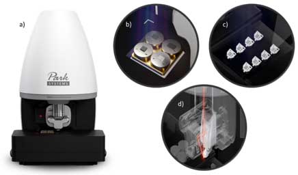
Figure 1. Park FX40 Atomic Force Microscope. (a) FX40 main-body, (b) multi-sample chuck showing kinematic mounting plates, (c) tip cassette for automated tip exchange (ATX), and (d) new beam-bounce scheme to measure cantilever deflection.
The purpose of an atomic force microscope (AFM) is to repeatedly and reliably measure surface topography in three dimensions with sub-nanometer resolution. Additional information such as electrical, magnetic, nanomechanical or chemical information can be obtained simultaneously, yielding a vast array of information from a single instrument. Sample preparation is minimal, if any, and cost of ownership is low compared to related techniques. Images can be obtained in air, liquids, and controlled atmosphere. This has made AFM’s indispensable tools in industrial and research applications. Before obtaining any AFM data, the user must select a suitable cantilever/tip (or probe), load it into the tool using tweezers, and align the optical detection system and viewing optics. This is followed by loading a sample and selecting one or more areas to image. The operator then has to select a basic imaging mode such as Non-contact or Tapping, tune the system, and manually guide the AFM tip to within detection range of the surface. To obtain valid surface information, the user must tell the AFM how to track the surface based often just on “visual” feedback. These rather complex procedures have prevented AFM from entering mainstream as it generally takes a very experienced person to obtain good, reproducible data.
Park Systems AFMs like the NX- or XE-series already addressed some of the challenges, such as using pre-mounted tips and a user-friendly interface that can help select imaging parameters based on objective boundary conditions and settings. However, the FX40 automates the whole imaging process thus removing the barrier for easily getting consistent data quickly. This is a necessary step for giving access to the fantastic nano-metrology information AFM can provide to a wider audience.
In addition to automating the imaging process, FX40's new optomechanical design yields an increase in data quality and measurement precision. The low noise level allows it to easily perform accurate nano-metrology on challenging samples. Even though counterintuitive, a challenge for AFM is often accurate data on large flat samples. Here, FX40 builds on the experience gained using cross-talk elimination on the previous generation of Park AFMs. The raw out-of-plane-motion (OPM) before image correction is < 2nm over 80µm scan range, enabling precise measurements without being impacted by common leveling artifacts. 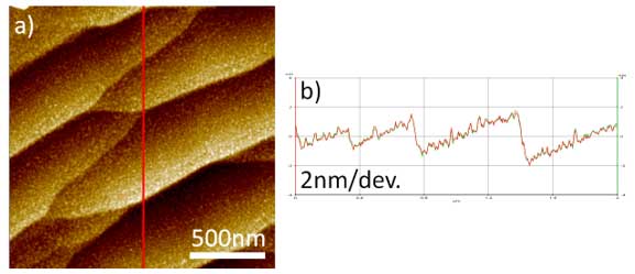
Figure 2. Low noise levels for accurate nano-metrology. a) Atomic terraces on sapphire, b) Linescan profile of sapphire. Steps with sub-nm features signals are perfectly matched in forward (red) and reverse scan (green).
In the following we describe the acquisition process for topographic images using four different samples to demonstrate the automation of Park FX40 including easy sample to sample navigation:
- The first in the set of samples is a semifluorinated alkane (F14H20) assembled on a silicon substrate (figure 8).
- The second sample is graphene on Boron nitride, a common 2D material system being studied for its electronic properties (figure 9).
- The third sample is a copolymer of styrene-butadiene-styrene (figure 10).
- The fourth and last sample is polytetrafluoroethylene (Teflon), a polymer with a vast number of industrial applications (figure 11).
In addition to topographic data, FX40 can acquire additional physical information of the sample and correlate with the topography. Four examples are depicted in figure 3: nanomechanical information such as modulus or adhesion information (Figure 3a), magnetic information including the possibility to study the sample under controllable external magnetic fields (Figure 3b), nanolithography (3c), and the measurement of electrical properties with high spatial frequency (3d), to list just a few.
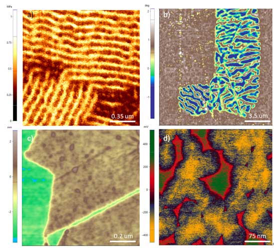
Figure 3. A small sample of FX40 Data acquisition modes. a) Young’s Modulus of block copolymers obtained by PinPointTM. b) Magnetic Vortex Cores in Cr/Ni/Mo alloy obtained by Magnetic Force Microscopy. c) Topography of divided graphene flakes. d) Surface Potential of Semifluorinated alkanes obtained by Sideband KPFM: Negative potential (yellow/blue section) identifies the alkanes relative to the substrate.
Experimental
The real-time operational scheme, from tip mounting to final imaging, is explained in the following outline: The whole process can be executed in three simple steps:
1. In the first step “ATX” (Automatic Tip Exchanger), the operator selects the cantilever for the imaging mode identified. Without additional user input required, FX40 automatically mounts the probe-tip, aligns the beam-bounce system using machine learning for optimal cantilever detection.
2. The second step “Sample'' allows the user to select the sample and desired initial imaging area using the two built-in high performance optical viewing systems. After successful selection, the AFM moves to the selected area, performs necessary tuning operations, and automatically approaches the sample. The build-in optical autofocus system allows for a tip-sample approach in seconds.
3. The next and final step starts the automatic AFM scan and data acquisition.
This technical note separates the process into discrete steps and explains the mechanism behind them.
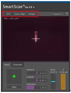
Figure 4. Part of the SmartScanTM Interface for FX40. “ATX” button in the top left corner enables the automatic-tip exchange. Auto align button focuses the cantilever, aligns the SLD and the photo detector. Sample button enables the sample navigation camera, allowing the user to select the desired sample.
Step 1: Auto tip mounting and beam alignment
In this step, the software identifies the probe type by reading the QR-codes on the chip carriers in the probe cassette. Once the chips have been identified, the operator can select the probe to use and FX40 automatically picks a probe from the cassette. After that, the FX40 finds the cantilever and superluminescent diode (SLD) and photodetector alignment are performed automatically.
The Park FX40 positions the SLD within the optical microscope; this innovative design ensures that the SLD beam is always focused at the center of the lens. Due to the fixed position of the SLD, centering the cantilever in the middle of the optics immediately aligns the SLD. To complete the beam-bounce alignment, embedded motors in the AFM head adjust the angle of the steering mirror, which automatizes the photodetector alignment process; all by 1 simple click. This automatization eliminates user error and ensures perfect operation every time.
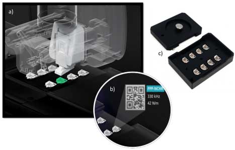
Figure 5. Automatic tip exchanger (ATX). a) View of automatic tip exchange slots image with cantilevers. b) Magnified rendering of QR codes that allows the system to recognize the selected probe and automatically upload the cantilevers profile. c) Probe cassettes can easily be removed and exchanged.
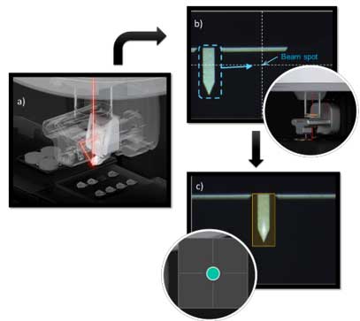
Figure 6. Optical cantilever alignment and laser beam detection. a) Park FX40 superluminescent diode beam path. b) Machine learning is used to center the cantilever. c) Centering the cantilever automatically aligns the beam-bounce system.
Step 2: Auto sample positioning
FX40 uses a dedicated sample view camera to navigate to the desired location. The "Sample" button shown in figure 4 opens the positioning panel and activates the sample view camera located above the sample chuck which can hold up to four individual samples. Once the desired initial imaging location is selected, the system immediately moves to the selected region (Figure 7). After selecting the desired imaging spot , FX40 executes a fully automated, fast tip-sample approach [3].
Step 3: Auto imaging
SmartScan Auto Image Mode is used to acquire the topographical data . This mode performs all the necessary imaging operations and intelligently selects the optimum image quality and scan speed. This ensures consistent data quality independent of operator experience level. Processes such as the cantilever frequency sweep, operations setpoint, scan speed or gain adjustment are part of the automatized procedures, reducing the time otherwise needed for manual user inputs and manipulation.
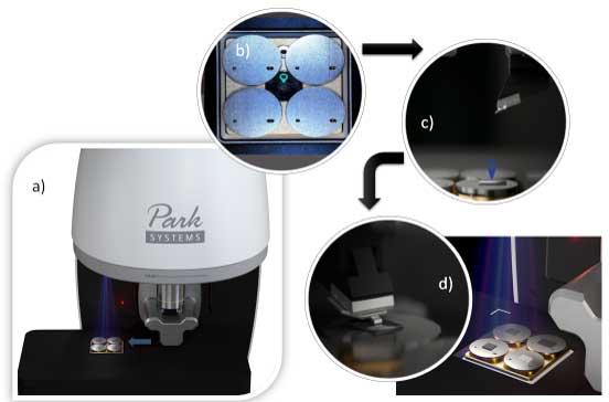
Figure 7. Sample navigation. a) Park FX40 main body with the multi-sample chuck kinematically locating the samples. b-d) Sample panel activates and allows the user to select the desired spot on the sample. The cantilever then moves to the user selected location and automatically approaches at the selected sample location. After completing data acquisition, the software secures the system by lifting the Z stage and turning the SLD off. The used probe returns to the ATX cassette if the operator does not plan to use it right away.
Results
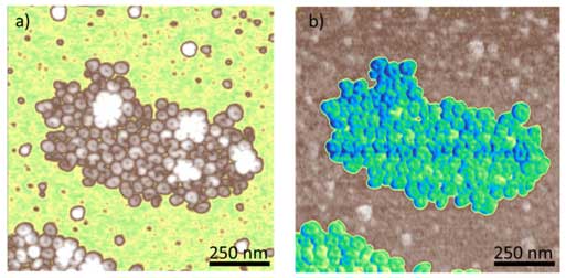
Figure 8. Semifluorinated alkanes on Si. (a) Topography image depicting the spiral morphology of the sample (vertical scale range 0 to 12 nm) and (b) Phase image of F14H20 alkanes (vertical scale range 0 to 6 degrees). The phase highlights additional sample details.
Thanks to the automation of FX40, the data in Figure 8 were acquired in a couple of minutes from start-to-finish. Figure 8 shows the high-quality topography obtained using a NCHR cantilever in non-contact mode, which clearly reveals a spiral superstructure of the F14H20 aggregates. After completing the image, the sample button was activated to navigate to the next sample: Graphene on h-BN. The same cantilever was used to obtain the topography and Moiré patterns information of the sample (Figure 9).
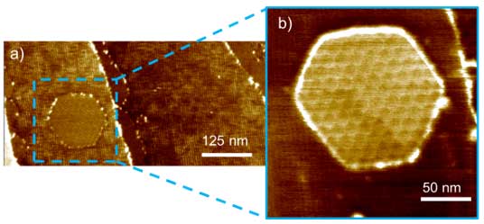
Figure 9. Moiré pattern observed on graphene on h-BN. a) Topography scan of graphene on h-BN, vertical scale 0 to 6 nm. b) Zoom in: Moiré pattern clearly visible, vertical scale 0 to 6 nm.
Figure 10. Styrene-butadiene-styrene (SBS) copolymer. a) Topography, vertical scale range 0 to 5 nm.
b) Corresponding phase showing the organizational structure, vertical scale range 0 to 5 degrees.
The same tip was used again to image sample #3. The phase image in Figure 10 highlights the composition of the sample. Finally, the tip was changed to a high-frequency tip and moved to scan location on the last sample on the multi-sample chuck. Figure 11 shows the molecular arrangement of the sample in topography and phase data.
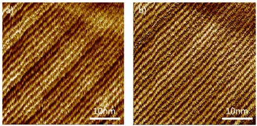
Figure 11. High Resolution Image of PTFE (Teflon). a) High resolution topography. Vertical scale range 0 to 3 nm b) Corresponding phase image. Vertical scale range 0 to 10 degrees.
Conclusion
This technical note demonstrates the innovative design, ease of operation, and superior imaging capabilities of the new Park FX40. This automatic AFM system can acquire high-quality images fast, using novel features such as machine learning and pattern recognition, QR-code based tip selection, and fully automatic tip exchange and alignment. Finally, FX40 can acquire precise data with its low signal-to-noise ratio and intuitive user interface. Park FX40 is a significant advancement in nanotechnology and metrology that will further innovation and discoveries across nanoscience and engineering fields.
References
1. Park SmartScanTM: Park AFM Operating Software: https://parksystems.com/products/operating-software/park-smartscan
2. Park Systems (2020). Probe Store. California, USA.: https://parksystems.com/service/probe-store
3. Park Systems Inc (2015). Revolutionary Park Systems SmartScan Automatizes the Atomic Force Microscope Imaging Process–High Quality Images at Click of a Button. California, USA.: https://parksystems.com/company/news/press-release/490-smartscan-automatizes-the-atomic-force-microscope-imaging-process
4. Park Systems Inc (2021). NCHR Cantilever. Probe Store. California, USA.: https://parksystems.com/service/probe-store