


Nanotech France 2022, the 7th edition of the international conference and exhibition, brings together leading scientists, researchers, engineers, practitioners, technology developers and policy makers in nanotechnology to exchange information on their latest research progress and innovation.

Join Alexander Klasen, Principal Scientist from Park Systems Europe at NanoTech France 2022 for his talk:
- ⏩ TALK TITLE: “Correlating the functional properties of graphene on the nanoscale”
- Thursday, 16 June, 10am CEST, Session III.A: Materials and Nanomaterials for Energy / Nanoelectronics/ Nanophotonics
ABSTRACT
Correlating the functional properties of graphene on the nanoscale
Alexander Klasen,1 Simonas Krotkus,2 Michael Heuken,2 Ben Conran,3 Ilka M. Hermes,1 Clifford McAleese,3 Xiaochen Wang ,3 Oliver Whear3
1 Park Systems Europe GmbH, Mannheim, Germany, 2 AIXTRON SE, Herzogenrath, Germany, 3 AIXTRON Ltd, Cambridge, United Kingdom
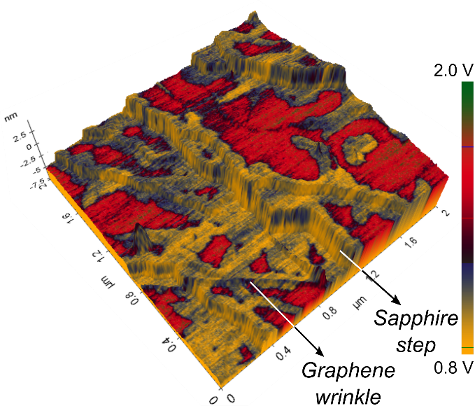
The industrial application of graphene in high-performance nanoelectronics requires wafer-scale fabrication, ideally on insulating substrates, and electronically uniform surface properties [1]. Therefore, real-space imaging of the graphene topography as well as mapping the electronic properties with a nanometer resolution is essential. Atomic force microscopy (AFM) not only visualizes surface topography, but can additionally resolve functional properties, such as surface potential and work function, adhesion and elasticity. Here, we investigated electronic and mechanical properties of a CVD grown wafer-scale graphene film on sapphire [2] via functional AFM techniques. Using sideband Kelvin probe force microscopy (KPFM) we were able to resolve a heterogeneous surface potential distribution with distinct contrast between the bulk film, graphene wrinkles as well as on the underlying sapphire terraces and step edges [3]. The surface potential distribution correlated with the mechanical behavior, including deformation and adhesion, which gave a distinct contrast on the same features, resolved via PinPoint nanomechanical AFM. The correlation of the surface potential and the sample’s nanomechanical response may originate from a delamination at step edges, affecting the local electronic properties. Especially the local change of the surface potential has to be considered when incorporating graphene in nanoelectronic devices.
Figure: 3D overlay of the graphene topography, which displayed wrinkles and underlying sapphire steps as indicated, with the surface potential imaged via sideband KPFM.
References
[1] S. J. Kim, K. Choi, B. Lee, Y. Kim and B. H. Hong, Annu. Rev. Mater. Res., 45 (2015), 63–84
[2] N. Mishra, S. Forti, F. Fabbri, L. Martini, C. McAleese, B. R. Conran, P. R. Whelan, A. Shivayogimath, B. S. Jessen and L. Buß, Small, 15 (2019), 1904906
[3] U. Zerweck, C. Loppacher, T. Otto, S. Grafström and L. M. Eng, Phys. Rev. B, 71 (2005), 12542