


 By Dr. Ardavan Zandiatashbar, Ph.D.,
Research Scientist Park Systems Inc., Santa Clara, California.
ESSENTIAL TOOL FOR HARD DISK MEDIA FAILURE ANALYSIS
Failure analysis engineers in data storage rely on atomic force microscope (AFM) as one of the key techniques for obtaining threedimensional information about the topological defects on hard disk media samples. This information is critical for proper identification of defects and eliminating defect sources. Although optical microscopy can provide a quick image of sample surface, the technique has limited resolution due to light wavelength. On the other hand, electron microscopy can provide higher resolution but it is essentially a destructive technique and provides only a twodimensional image. AFM provides the highest vertical and lateral resolution and provides a three-dimensional topography of the sample surface [1]. The conventional AFMs were known to have limited throughput and tip life since imaging was performed in destructive mode. To address these limitations of AFM, Park Automatic Defect Review (ADR) AFM has been developed and introduced in mid 2000s for a non-destructive high throughput 3D imaging of defects. This solution was widely accepted and welcomed in failure analysis (FA) labs globally. In this article we introduce the latest generation of ADR-AFM. The new ADR-AFM utilizes enhanced vision technique to facilitate locating defect of interest (DOI). This solution carries the commercial name of Park NX-HDM.
The main objective of the FA lab for hard disk media is studying the defects and investigating the possible defect sources to improve yield management. For this purpose, defect study consists of two main steps: defect inspection, and defect review. In defect inspection, an inspection tool searches the media surface using optical, electron beam, or magnetic probe to find the location of the defects. The output is a map of defects which indicates their distribution over the sample surface. The defect map can also be used for locating the DOI for further investigation. Although the inspection tools have high throughput and are able to test several samples per hour, they are limited in resolution and are not suitable for characterizing each defect effectively. Therefore some of defects are selected for defect review and detailed characterization. In defect review, defects of interest are characterized to obtain a high resolution image and classified accurately. The defect review process relies on techniques that can provide high resolution topographical information about each defect. The examples for defect review techniques are AFM and S/TEM. Unlike inspection tools, the review techniques are relatively slower and need to accurately locate DOI for imaging.
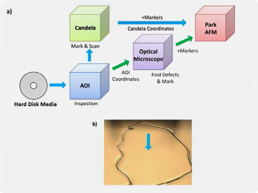 Figure 1.
a) Current process of defect inspection and review for hard disk media. The green path shows the process path for conventional AFMs. The blue path shows the process with the first generation of Park ADR-AFM.
b) A defect on hard disk media sample which is marked by a surrounding scratch. The defect is hardly visible in optical vision of AFM.
Locating DOI is the major challenge for defect review tools. There is a difference between the coordinates of DOI on the stage of inspection tool versus its coordinates on the stage of review tool. This difference is referred to as stage error. The stage error is generally larger for in-house inspection tools (e.g. AOI, Tester) comparing to commercial inspection tools (e.g. KLA-Tencor Candela). The process of defect inspection and review is depicted schematically in Figure 1a. In the past and before introducing ADR-AFM, manual AFM was used for imaging DOI. To facilitate locating DOI in manual AFM, FA engineers initially marked every single defect. As shown in Figure 1a hard disk media is inspected with an automated optical inspection (AOI) tool which is the most commonly used equipment in mass production and the map of defects is generated. Then the disk is investigated by an optical microscope for locating and marking each DOI. Marking defects was done by making observable scratches around each defect to facilitate finding it through the optics of AFM (Figure 1b). This process path is shown by green arrows in Figure 1a. This included performing multiple survey scans to find DOI. This method had a low throughput of 10 defects per day in best scenario. In addition, conventional AFMs were using destructive scanning method (tapping mode), therefore, tip life was limited due to performing multiple large survey scans that was required for finding each defect and the whole process resulted in high cost of ownership.
The first generation of Park ADR-AFM had been introduced in order to address the limitations of conventional AFMs in the defect study process. This solution provided two major advancements comparing to conventional AFMs. First, it has a significantly improved throughput up to 10 defects per hour as a result of automated process. Since the system was operated by automated software, the user did not need to be present during the scan. Hence the system could continue locating and imaging a large number of defects on its own (even overnight). This improved the throughput of an AFM system significantly. Second, the imaging was performed in non-contact mode. Using non-contact mode imaging extended the tip life, which is critical for automated defect review process and getting consistent data. Therefore a single tip could be used for a significant number of images without user being present.
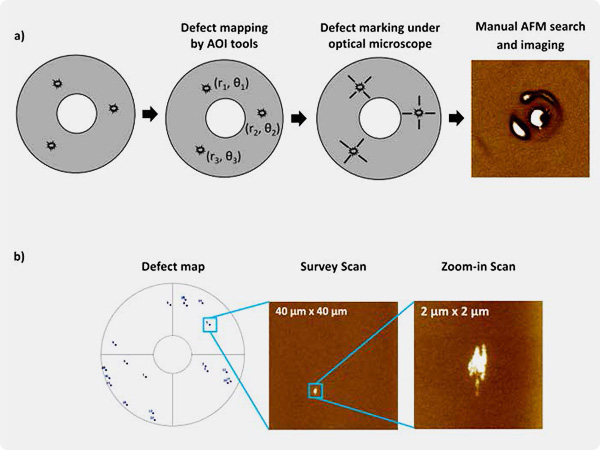 Figure 2.
The AFM based defect study process is schematically shown for a) manual AFM, b) ADR-AFM. In ADR-AFM, locating the defect from defect map, survey scan, final zoom-in scan are performed automatically by the system.
The ADR-AFM process is depicted in Figure 2 and compared to conventional process using manual AFM. In conventional AFM imaging (Figure 2a), the sample surface was first searched with an inspection tool. This was followed by marking the DOI on the surface using optical microscope. After laborious efforts of marking each DOI, the sample was brought to AFM for imaging. Finding the defect in AFM required visual search in vision and followed by multiple low and high magnification scans (green path in Figure 1a). In ADR-AFM, DOI coordinates from inspection tool are initially imported which is followed by coordinate alignment. After this step, automated software moves the tip to each defect, performs a survey scan, images the defect, and classifies the defect automatically. With ADR AFM throughput of defect review increases up to 100 defects per day. In addition, since this process is fully automated, engineer do not need to stand by and operate the system during the runs which frees up their time and boosts productivity.
The survey scan size of old Park ADR-AFM was selected based on the stage error of the inspection tool used to generate defect maps. A 40 μm × 40 μm survey scan was typical to cover for a stage error up to 20 μm between AFM and Candela. Since the stage error of AOI tools are very large (≥ 50 μm), using a linkage tool (e.g. Candela) with smaller stager error was necessary in order to have the process of defect study complete as shown by blue path in Figure 1a. A set of 16 markers were added to each wafer before the inspection run by Candela to be used for sample alignment in Park ADR-AFM.
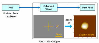 Figure 3.
An example of enhanced vision image and how it facilitates linkage between the AOI tool which has larger stage errors and Park ADR-AFM.
The new generation of Park ADR-AFM is introduced recently for both hard disk media and 300 mm wafers [2]. Bright field enhanced vision is introduced in the new generation of Park ADR-AFM. It provides the ability to observe defects in ADR-AFM optical field of view (FOV). Bright field enhanced vision utilizes differential frame averaging technique and precise movement of sample by decoupled XY scanner to observe small defects that are hardly visible through regular optics of the system. Decoupled XY and Z scanner structure of Park ADR-AFM enables using differential frame averaging by collecting optical images of the sample surface at two precisely separated positions of XY scanner. The differential image of the frames of sample surface collected at two different positions enhances the contrast of small defects and makes them visible in optics of ADR-AFM. Since the FOV of ADR-AFM is larger than the maximum survey scan size, enhanced vision enables the ADR-AFM to accommodate even larger stage errors of inspection tools (Figure 3). Collecting a typical bright field enhanced vision image takes between 1 – 30 sec for each defect.
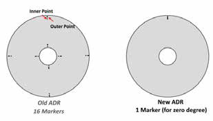 Figure 4.
The schematic shows the sample alignment process in the first (left) versus the new (right) generation of Park ADR-AFM. In the latest Park ADR-AFM only one marker is needed to indicate zero-degree location of hard disk media samples.
In addition to bright field enhanced vision, a new sample alignment algorithm is developed to facilitate the linkage between the ADR-AFM and inspection tools. In the first generation of ADR-AFM, a sample alignment by using 16 markers was needed to align the sample on the ADR-AFM stage. The coordinates of 16 markers were generated by Candela, and were matched with the coordinates of ADR-AFM stage. In the next generation of ADR-AFM, only one marker is needed for sample alignment. The new alignment process consists of one coarse and one fine alignment step. In the coarse alignment, three points at the circular perimeter of the hard disk media sample is used for finding the sample center, and a zero-degree marker is used for finding the rotation of the sample. In the fine alignment step, ADR-AFM uses few larger defects for minimizing the remaining positioning errors by utilizing enhanced vision. The new alignment process is faster and more convenient for sample alignment comparing to the first generation of ADRAFM. In addition, it can also be used as a tool for evaluating the stage error of AOI or other inspection tools (Figure 4).
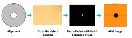 Figure 5.
The new ADR-AFM process with newly introduced dark field enhanced vision for hard disk media with reflective surface.
Dark field enhanced vision is introduced in the latest generation of Park ADR-AFM. The new dark field enhanced vision enables AFM to observe defects in a short time on reflective surfaces by collecting the light scattered due to surface defects. For this purpose, a new hardware module is developed and implemented in the AFM system. In this module a laser beam is emitted to the location of interest on the sample. The beam angle of incidence is larger than zero degrees such that the direct beam reflection is not collected by the on-axis optics of ADR-AFM. For a reflective sample, majority of laser beam is following the expected reflection path with similar angle of incidence. In case the surface a topological defect is present on the sample surface, part of the laser beam will be scattered in different directions other than the regular reflection path and are collected by on-axis ADR-AFM optics. The collected frame is an image of the surface with collected scattered light from the defects. Examples of standard optical and dark field enhanced vision images are shown in Figure 5. The upgraded ADR-AFM process with dark field enhanced vision is presented schematically in Figure 5. In the new process, after the sample alignment, ADR-AFM goes to defect location, recognizes the defect using dark field enhanced vision (without AFM scanning), and performs the imaging, analysis, and classification. The new process enables ADR-AFM to minimize the positioning error. As a result the required survey scan is also minimized and the throughput is increased. As a result, it enables ADR-AFM to accommodate defect maps from AOI systems that have large stage errors. The ability to see the defects by enhanced vision enables ADR-AFM to be used as the reference tool for evaluating the stage errors of different inspection tools.
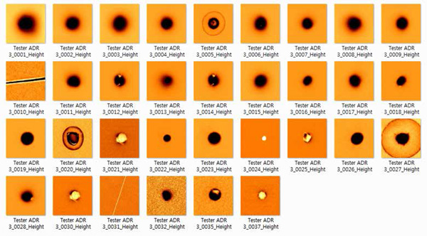 Figure 6.
The results of performing ADR-AFM on a 95 mm hard disk media samples for a set of defects reported by an in-house inspection tool. 33 defects out of 37 was found and imaged by ADR-AFM.
The results of a defect review by ADR-AFM on a 95 mm hard disk media sample are shown in Figure 6. The defect coordinates were provided by an in-house inspection tool with large stage error (> 50 μm). Dark field enhanced vision has been used for locating the defects. As the result, ADR-AFM was able to find 33 out of 37 defects successfully using the addition of enhanced vision. The defects are classified to two groups of pit and bump by ADR-AFM. An example of each group is depicted in Figure 7. In this figure dark field enhanced vision images and AFM images of defects are shown. ADR-AFM was able to find defects with vertical dimension as low as < 3nm.
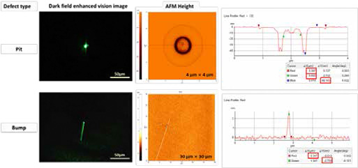 Figure 7.
Representative pit and bump type defects on a hard disk media samples which were found and imaged by ADR-AFM. The dark field enhanced vision images are shown side by side the AFM images and selected profiles of the defects.
In summary, the latest generation of Park ADR-AFM is equipped with new bright field and dark field enhanced vision modules. The bright field enhanced vision utilizes frame averaging technique and ADR-AFM’s decoupled XY scanner to obtain a high resolution optical image of the sample surface to help locating the DOI. Dark field enhanced vision is enabled by collecting the scattered laser signal by the on-axis vision of ADR-AFM and enables detecting defects on the surface of reflective surfaces. Park ADRAFM uses non-contact mode imaging and therefore is imaging the samples in a non-destructive method. Park ADRAFM with enhanced vision modules and updated alignment algorithms is used for high throughput AFM based defect review. Additionally, ADR-AFM with enhanced vision is a potential reference tool for evaluating the stage error for inhouse inspection systems that are being developed or maintained.
REFERENCES
[1] Smith, G. T., Industrial Metrology: Surfaces and Roundness, Springer, London, 103-105 (2002).
[2] Ardavan Zandiatashbar et al., "Highthroughput automatic defect review for 300mm blank wafers with atomic force microscope," in Proc. SPIE 9424, Metrology, Inspection, and Process Control for Microlithography XXIX, 2015, p. 94241X.