


AFM Failure Analysis for Semiconductors and Electronic Devices
SSRM AFM for Optimal Results in Semiconductor Failure Analysis
The High Vacuum Scanning Spreading Resistance Microscopy (SSRM), available on Park NX-Hivac, enables 2D carrier profiling of next generation devices and measures the high resolution SSRM image under high vacuum conditions to improve production yield. The high vacuum SSRM measurements show much higher accuracy and resolution than in ambient conditions. Thanks to the very high sensitivity and responsiveness to the current signal, SSRM ensures accurate measurements and repeatability, providing a high-level tool for semiconductor failure analysis. In addition, the integration of a new operational AFM mode called PinPoint™ with SSRM enables acquiring topography, electrical and mechanical property data simultaneously. Furthermore, operating in an approach-retract manner greatly reduces friction and tip wear compared to standard SSRM.
SSRM enables:
• higher sensitivity and resolution in high vacuum compared to the ambient conditions,
• higher accuracy and repeatability of the measurements,
• acquisition of multiple properties simultaneously (electrical, mechanical, topography),
• longer tip lifetime and reduced sample damage when performed in PinPoint™ mode,
• frictionless imaging when performed in PinPoint™ mode.
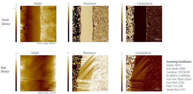
Device-Failure Analysis by SSRM
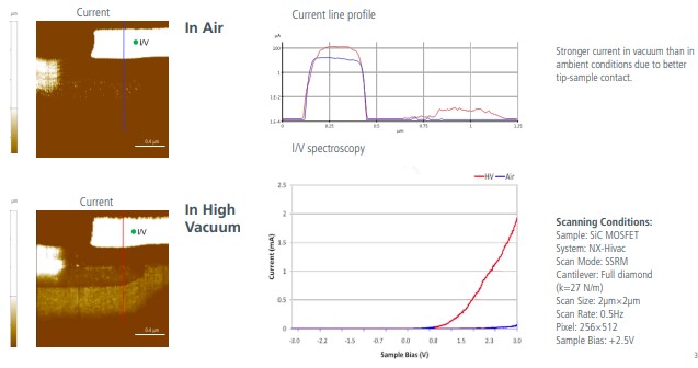
SSRM in Air vs. High Vacuum
Conductive AFM as AFM Failure Analysis for Electrical Devices
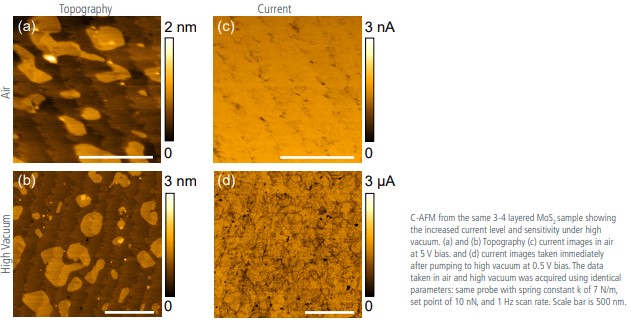
Conductive AFM (C-AFM) simultaneously measures topography and electrical properties (conductivity) of samples by using the AFM tip as a nanometer-scale electrical probe. More specifically, it monitors the current flow between the conductive tip and sample, and when the bias is applied. At the same time, it records the cantilever deflection as the tip scans over the sample surface. The measurements can be performed in contact mode, tapping mode, or PinPoint™ mode. The latter one operates in an approach-retract manner, ensuring a frictionless operation which eliminates the lateral force caused by continuous tip-sample contact. The control over the contact time and contact force between the tip and sample surface allows acquisition of accurate and reproducible data, and thus, it is a key feature for the defect testing of continuously smaller electrical devices. C-AFM in High Vacuum for improved material analysis Performing C-AFM measurements in High Vacuum (HV) improves the quality of the image significantly. In particular, the measured current increases by three orders of magnitude in comparison to ambient conditions and features high homogeneity. The current maps taken in HV show remarkably more details than taken in air.
C-AFM enables:
• obtaining high quality data for both topography and current measurements,
• high resolution imaging due to the elimination of frictional force when performed in PinPoint™ mode,
• accurate mapping of the current variations at the surface due to ability to control the contact force and time when performed in PinPoint™ mode,
• homogeneous and higher current signal when performed in High Vacuum in comparison to ambient condition.
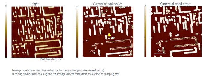
Failure Analysis of Semiconductor Device by C-AFM
C-AFM in Air vs. High Vacuum
Electrical Characterization of Semiconductor Devices Using Scanning Capacitance Microscopy (SCM)
Characterizing electrical properties with high spatial resolution is a key in understanding the functionality of a semiconductor device. Scanning Capacitance Microscopy (SCM) is a powerful method to characterize semiconductor devices due to its non-destructive scanning ability, and high accuracy in measurements with nanoscale features. SCM enables simultaneously acquiring topography and electrical property data with great lateral resolution and high contrast mapping, without changing the tip. In Semiconductor Manufacturing SCM provides dopant profiles which help in failure analysis and enables design advancement. In addition, Park’s new QuickStep SCM mode provides accurate dopant profiles of semiconductor device structures five to ten times faster than other competing SCM atomic force microscopy systems. It guarantees the fastest scan speed without compromising signal sensitivity, spatial resolution or data accuracy. For device characterization, SCM provides the unique ability to measure qualitative 2D dopant profiles.
SCM enables:
• non-destructive scanning ability,
• longer tip lifetime and no sample damage thanks to the low force tip sample interaction,
• ultra-fast scan speed with high signal sensitivity, spatial resolution and data accuracy
• accurate measuring 2D dopant profiles,
• high productivity due to minimized drift effects during sequential zooming to the target location.
Nanoscale Failure Analysis by SCM
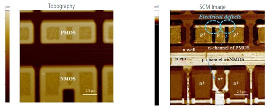
Topography (Left) of PMOS and NMOS transistors
SCM data (Right): Lowly doped p- type region is shown in bright colors and n- type dopant is shown in dark colors. Highly doped p+type or n+ type areas show intermediate color contrast for example yellowish color.
QuickStep SCM vs. Conventional SCM
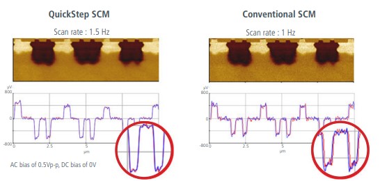
Higher Quality SCM Image - High Throughput QuickStep Scan is 5~10 times faster than conventional SCM scan with no compromise of signal sensitivity, spatial resolution, or data accuracy.
Failure analysis by Scanning Thermal Microscopy (SThM)
Scanning thermal microscopy (SThM) investigates thermal properties of various nanostructured materials. Due to the capability of detecting failures caused by the hot spots on the sample surface, SThM has become a powerful tool to analyze semiconducting materials and devices at high spatial resolution. The key part of SThM measurements are nanofabricated thermal probes with resistive elements to achieve unprecedented high spatial and thermal resolution and sensitivity with a unique signal detection scheme.
SThM operation modes:
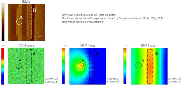
• Temperature Contrast Mode (TCM) - measures the temperature variations on a sample surface
• Conductivity Contrast Mode (CCM) - measures variations of thermal conductivity on a sample surface
SThM can cover the temperature range of RT ~ 150 °C with a temperature resolution of 0.1 °C.
SThM enables:
• measuring localized thermal properties (temperature, local thermal conductivity),
• unprecedented high spatial and thermal resolution,
• sensitivity with a unique signal detection scheme.
SThM - Si nanowire on glass
SThM - Pole-Tip-Recession of HDD Head
Automatic Defect Review as an inline method for defect review in Semiconductor Industry
Addressing the continuously decreasing size of semiconductor devices in modern technology, AFM provides a high-resolution and non-destructive analysis method for defect review at the semiconductor industry. The Automatic Defect Review (ADR) AFM, introduced by Park Systems, is an automated process, which simplifies and speeds up the previously time-consuming workflow for AFM in the defect characterization. Due to the diffraction limit of visible light, the conventional automatic optical inspection (AOI) cannot achieve a sufficient resolution in that range, which impairs quantitative imaging and consequent classification of defects. The ADR AFM, on the other hand, visualizes defects in three dimensions at the nanometer-resolution characteristic for AFM. Especially for defect sizes in the law nanometer-range, ADR AFM complements conventional AOI, with the high vertical resolution of AFM facilitating a reliable and three-dimensional defect classification. The non-contact measurement mode ensures non-destructive surface characterization and prevents wear of the AFM tip, which guarantees that high resolution is maintained in many consecutive measurements.
ADR AFM enables:
• simple and time-saving workflow for defect characterization in AFM,
• fully automated defect characterization of four to ten defects per hour,
• visualization of defects in three dimensions at nanometer-resolution,
• non-destructive surface characterization and low tip wear due to non-contact measurement.
Automatic Optical Inspection (AOI) vs. ADR AFM
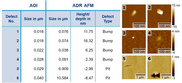
Direct comparison of the defect sizes determined with automatic optical inspection (AOI) and ADR AFM in the table on the left side. The according AFM topography scans of all six defects are shown on the right. Protruding defects are named bump, indenting defects are named pit.
ADR AFM vs. ADR SEM
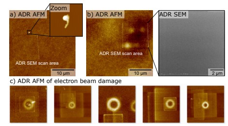
Comparison between ADR AFM and ADR SEM, a) AFM image of bump defect missed previously by ADR SEM. The ADR SEM scan area is visible as rectangle in the AFM topography scan. b) Imaging of a defect with a low height (0.5 nm), which was not resolved by ADR SEM. c) Examples of electron beam damage on the wafer-surface following ADR SEM measurements, visible as rectangular areas around the defects.