


Nano-pipette based scanning probe microscopy
Introduction
Since atomic force microscopy (AFM) has been developed1, various applications of nanotechnology were established that led to technological advances in many fields of science. Using decoupled XY and Z scanners, three-dimensional information of sample surfaces can be obtained. For that, a cantilever with a tip diameter of a few nanometers scans a sample surface and detects force originating from interactions like van der Waals forces and Pauli repulsion between the tip and the sample surface. While AFM provides access to a pool of information on a variety of samples with nanometer resolution, it is very challenging to image very soft samples like biological samples in a liquid environment. Because of unexpected physical contact of AFM tip on the sample surface, small and fragile structures can be dragged or scratched. The AFM tip mechanically interacts with the living cell and might deteriorate its structural features, changing the living cell, if not killing it directly. In order to be a suited tool for imaging delicate biological samples, it must meet several requirements. At first, it should be able to acquire images in True Non-contactTM. Second, it needs to have stable feedback during imaging, and lastly, the imaging operation must be simple and easy. To address these requirements, scanning probe microscopy (SPM) techniques using nano-pipettes as probes have been developed. Although nano-pipettes have an inner diameter of approximately ~100-200 nm (Figure 1) and therefore offer not the same spatial resolution as general AFM tips, nano-pipettes enable stable non-contact measurements in liquids without damaging soft samples. Also, with inner diameters ranging from tens of nanometers to micrometer size, we have a variety of different nano-pipettes at our disposal to customize our experiments according to the respective purpose.
In this application note, we review SPM techniques using nano-pipettes as probes. Scanning ion conductance microscopy (SICM) is used for imaging the surface of biological samples, especially live or fixed cells2,3. SICM-SECM4-7, which combines SICM technology with scanning electrochemical microscopy (SECM)8 technology to simultaneously measure the morphology and electrochemical (EC) response of the sample surface, and scanning electrochemical cell microscopy(SECCM)9 , which can measure the surface EC response in liquid by creating small isolated droplets that allow for a more localized EC measurement.
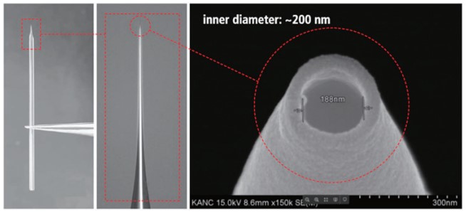
Figure 1. Optical and scanning electron microscopy(SEM) images of a pulled nano-pipette.
SICM
SICM is a resourceful SPM method for molecular biology and material science research, as SICM ensures non-contact imaging and works in liquid medium containing ions. As shown in figure 2, the fundamental operation of SICM relies on an ion current that flows between a pipette electrode and a bath electrode.
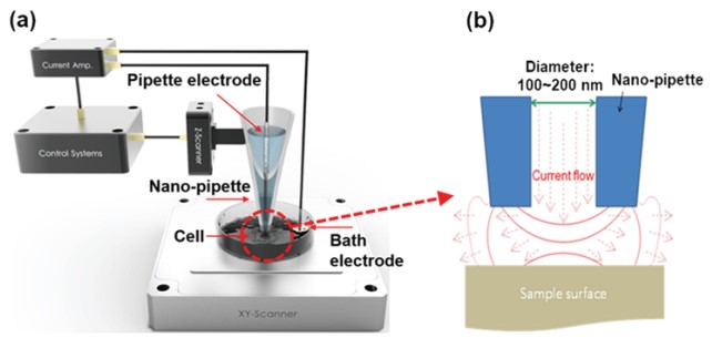
Figure 2. Schematic image of SICM (a) and current flow between nano-pipette end and sample surface (b).
When the nano-pipette is far away from the surface, the current is mainly determined by the diffusions of ions between the pipette electrode and the liquid medium. This diffusion depends on different factors like the inner diameter of the nano-pipette tip end, the ion concentration of the liquid medium, and the ion mobility. When the tip of the nano-pipette approaches the surface, the ion diffusion is spatially restricted, which result in a smaller ion current. Accordingly, this ion current is used as a feedback signal to maintain a constant distance between the nano-pipette and the sample. Since not any cantilever deflection but a decreasing current is used as the feedback signal, SICM can operate without any physical contact between the nano-pipette and the surface. During imaging, the current signal is always kept maintaining about only 1~2 % current reduced distance by feedback system (Figure 3). Since changes in the ion current can be measured with high sensitivity, the feedback loops ensures a contact free measurement that is essential to image soft biological samples like living cells.
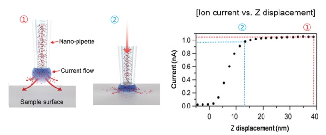
Figure 3. Current signal changes according to the distance between nano-pipette tip end and sample surface. The current signal changes according the to the distance between tip of the nano-pipette and the sample surface. 1 (red) corresponds the unrestricted diffusion current and large distance between nano-pipette end and sample surface. 2 (blue) corresponds to the restricted diffusion current as the nano-pipette end and sample distances get closer.
Figure 4 shows a representative measurement of a ciliated cell in the tracheal tissue of a rat to highlight the technical potential of SICM for cell imaging. SICM is able to acquire the complicated cell morphology in high magnification and without single contact to the sample surface, which would otherwise deform the cell. Also, the SICM can image a cell in physiological conditions which is necessary to ensure, that the measurement conditions do not alter the cell morphology. In contrast, SEM requires high vacuum, which probably isn’t the ideal environment for living things. Moreover, SICM can measure absolute heights, which are inaccessible with SEM. As shown in the SICM image in figure 4(a), cells can spread their cilia to surrounding cells to connect and form a complex network structure. This measurement clearly demonstrates the unique capability of SICM to acquire the surface topography even on complicated cell structures in liquid.
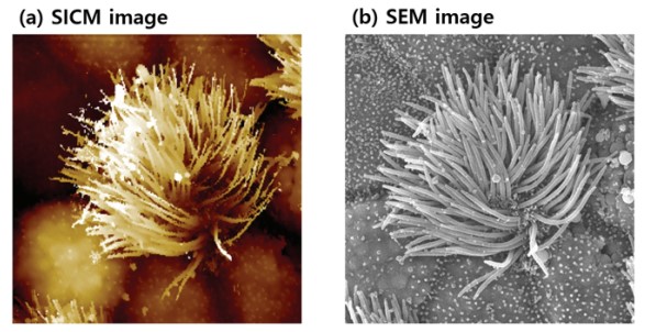
Figure 4. Ciliated cell in tracheal tissue of rat imaged by SICM in liquid condition (a) and SEM in vacuum condition (b). Image courtesy: Prof. Ushiki, Niigata University, Japan
SICM-SECM
SICM is a promising technique for biological sample imaging with no damage to the sample surface but, it is difficult to measure the EC response with only the current signal of the SICM. Normally, SECM is the option for EC response measurement. SECM employs a micro- or nanoelectrode, termed as the tip, to scan in the vicinity of a substrate. The bath solution consists of supporting electrolytes and an electrochemically active species. During a SECM experiment, the tip is biased at a sufficient potential such that the electrochemical active species will either be oxidized or reduced at the tip. By measuring the faradaic current, quantitative electrochemical information of the interfacial region will be obtained. However, feedback-controlled pipette positioning is complicated by the different faradaic current behavior over conductive and insulative substrates so, topographical information is not included in SECM output (Figure 5). To overcome the limitations in SICM and SECM, an alternative approach, hybrid SICM-SECM, has been developed. In SICM-SECM operation, the pipette-sample distance can be controlled via the SICM compartment, and the EC activity can be measured via the SECM compartment, enabling truly independent concurrent topographical and electrochemical imaging.
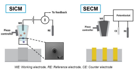
Figure 5. Schematic views of SICM and SECM
To perform simultaneous measurement of both topography and EC response, a specially designed nano-pipette is required, called ultramicroelectrode (UME). First, a nano-pipette with a 100 nm inner diameter is coated with a 10 nm Cr adhesion layer, followed by a 200 nm Au layer by thermal evaporation. Next, chemical vapor deposition of parylene C is performed such that the Au-coated nano-pipettes are completely covered by parylene C. Finally, a focused ion beam (FIB) is used to expose the nanopore and the Au crescent. After the FIB miling, final inner diameter of UME is approximately 200 nm. The exposed Au region detects the EC response while the UME tip end collects ion current signal for height imaging (Figure 6).
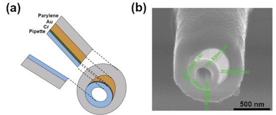
Figure 6. Schematic view of the cross section of a UME (a), SEM image of the tip of a UME (b).
For SICM-SECM imaging, firstly, the cyclic voltammetric (CV) curve is measured by a combined potentiostat. CV is a widely used electrochemical technique for electrochemical response studies and quantitative analyses. It measures electrochemical reactions taking place at the electrode surface using a current response while applying bias to the working electrode as a circulating potential in the presence of a chemical species capable of reversible oxidation/reduction. After immersing the UME in the buffer (Figure 7-Step 1), a CV curve is measured and it can be confirmed that the SICM-SECM is operating properly (Figure 7-Step 2). The UME approaches the sample surface (Figure 7-Step 3)and measures the CV again on the sample surface (Figure 7-Step 4). Then, EC response on the sample surface can be monitored. After checking the bias where the EC response occurs based on the CV result on the sample surface, the SICM-SECM image is performed while giving the corresponding bias (Figure 7-Step 5).
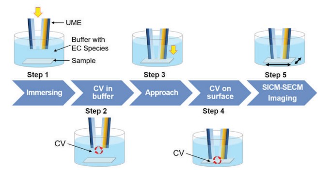
Figure 7. SICM-SECM imaging process.
Figure 8 indicates CV curves on Au/SiO2 stripe structure sample taken with the Au crescent electrode in a bulk solution containing 100 mM KCl + 10 mM Ru(NH3)6 3+ (Figure 8(a)) and after approach (Figure 8(b)). For 10 mM Ru(NH3)6 3+, starting from ~0.15 V, the reduction reaction takes place, and as the potential is ramped up, at ~-0.5 V, the electrochemical reaction is diffusion-controlled and a steady-state current is reached. From the CV data, a steady-state current was reached at -0.5 V, and, thus, the bias applied to the Au electrode at -0.5 V should show dominant contrast of EC response on Au/SiO2 region.
Figure 8. CV mapping process
Figure 12 shows an example of AFM and SECCM measurement on HOPG/ITO substrate to determine surface morphologies and to map EC signal contrasts of these two different materials. The regular AFM measurement and the SECCM measurement were conducted on the same area. All SECCM mappings images were obtained using a 500 nm inner diameter nano-pipette, 10 mM Ru(NH3)6Cl3, 100 mM KCl supporting electrolyte, and a 1 V/s scan rate. Using the confined meniscus contact on HOPG/ITO substrate, as the working electrode, nano-scale imaging could even distinguish the EC signal of the graphene basal plane, multi-layered graphene, and graphene with a conductive substrate. Different layers and step edges were visible in the height image that well align with distinctive features in the SECCM mapping image visualizing different EC activities of different graphene layers and step edges.
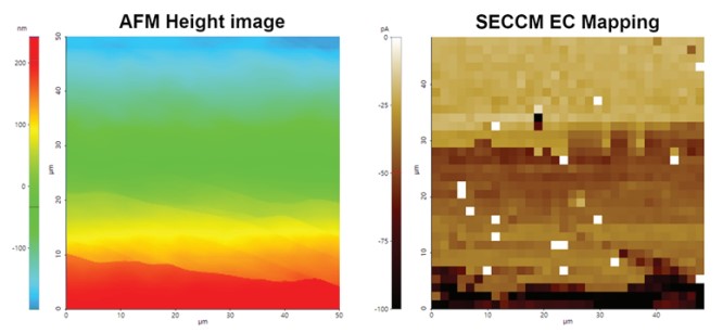
Figure 9. AFM image and EC response mapping by SECCM on HOPG/ITO sample.
Conclusion
In this application note, SPM techniques using nano-pipettes were investigated, which are, SICM, a non-destructive technology specialized for very soft samples, SICM-SECM that can measure EC activity together with SICM technology, and SECCM that can measure EC activity in ambient conditions. As shown in Table 1, each technique has its characteristics, and an appropriate technique should be selected and measured according to the measurement environment and purpose. In general, Although nano-pipette based techniques do not achieve the same spatial resolution as AFM because the inner diameter of the nano-pipette is more than tens of nm. However, nano-pipette based SPM techniques have the advantage of being able to cover applications that are difficult to apply AFM, so they are being used in various fields such as biology, electrochemistry, material science, and battery research.
| SICM | SICM-SECM | SECCM | |
|---|---|---|---|
| Working Principle |
Topography Feedback by ion current change according to distance |
Electrochemical property monitoring between UME and sample with topography |
Meniscus between tip and sample enables EC study in air |
| Probe | Nano-pipette | UME | Nano-pipette |
| Signal | Ion current | Faradaic current and ion current |
Faradaic current |
| Environment | In liquid | In liquid | In ambient (The EC reaction takes place in the meniscus.) |
| Remark | Topography and ion current images |
Simultaneous measurement of both topography and electrochemical property |
Electrochemical property in air, Easy setup and measurement |
| Typical experiment |
Topography of soft biological samples |
Local EC characteristics of catalysts or electrodes |
Table 1. Comparisons between nano-pipette based SPM.
References
1. Binnig, G., Quate, C. F., & Gerber, C. (1986). Atomic force microscope. Physical review letters, 56(9), 930.
2. Korchev, Y. E., Bashford, C. L., Milovanovic, M., Vodyanoy, I., & Lab, M. J. (1997). Scanning ion conductance microscopy of living cells. Biophysical journal, 73(2), 653-658.
3. Chen, C. C., Zhou, Y., & Baker, L. A. (2012). Scanning ion conductance microscopy. Annual Review of Analytical Chemistry, 5, 207-228.
4. Y. Takahashi, A. I. Shevchuk, P. Novak, Y. Zhang, N. Ebejer, J. V. Macpherson, P. R. Unwin, A. J. Pollard, D. Roy and C. A. Clifford, Angew. Chem. Int. Ed., 2011, 50, 9638-9642.
5. Y. Takahashi, A. I. Shevchuk, P. Novak, Y. Murakami, H. Shiku, Y. E. Korchev and T. Matsue, J. Am. Chem. Soc., 2010, 132, 10118-10126.
6. D. J. Comstock, J. W. Elam, M. J. Pellin and M. C. Hersam, Anal. Chem., 2010, 82, 1270-1276.
7. R. Thakar, A. E. Weber, C. A. Morris and L. A. Baker, Analyst, 2013, 138, 5973-5982.
8. Bard, A. J., Fan, F. R. F., Kwak, J., & Lev, O. (1989). Scanning electrochemical microscopy. Introduction and principles. Analytical Chemistry, 61(2), 132-138.
9. Ebejer, N., Güell, A. G., Lai, S. C., McKelvey, K., Snowden, M. E., & Unwin, P. R. (2013). Scanning electrochemical cell microscopy: a versatile technique for nanoscale electrochemistry and functional imaging. Annual review of analytical chemistry, 6, 329-351.