


Capturing conductive ferroelectric domain walls
Ilka Hermes and Andrea Cerreta1 1 Park Systems Europe, Germany
Introduction:
Ferroelectric materials typically feature wide band gaps and are therefore classified as insulators. They carry a spontaneous electrical polarization that exists in two or more orientation states and can be switched by applying an external bias. Areas that feature a uniform polarization orientation are called ferroelectric domains, separated by domain walls. These domain walls can be charged, if the polarization orientation of the two adjacent domains features a normal component with respect to the domain wall. For example, domains with a 45° polarization orientation may display positive 90° head-to-head walls or negative 90° tail-to-tail walls (Figure 1a). To compensate the bound domain wall charge and thereby lower the consequently increased energy, free electronic or ionic charge carriers accumulate at charged domain wall.1 The high density of free electronic charges and/or the ionic doping at domain walls lead to localized two-dimensional conductivities approaching those of metals.2–4 This 2D conductivity sandwiched between insulating domains and the possibility to tailor the domain wall arrangement as required makes conductive domain walls attractive systems for nanoelectronic applications.2
To image ferroelectric domain patterns and the position of domain walls on the nanoscale, piezoresponse force microscopy (PFM), featured in all of Park Systems’ NX and FX research atomic force microscopes (AFM), is ideally suited. In PFM, a conductive cantilever scans the surface in contact mode, while an AC voltage is applied between tip and sample. This AC voltage induces a periodic sample oscillation that leads to a periodic deflection of the cantilever during the scan. This sample oscillation is called piezoresponse, which captures the domain arrangement, polarization orientation, and piezoelectric behavior in PFM phase and amplitude. An AC excitation frequency close to the contact resonance of the cantilever can improve the signal-to-noise ratio of the piezoresponse for the characterization of sensitive materials or thin films.5 By correlating PFM domain imaging with conductive atomic force microscopy (C-AFM), the researcher can directly correlate local 2D conductivity with the position of charged ferroelectric domain walls.
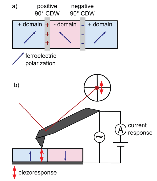
Figure 1: a) Example of positive and negative 90° charged domain walls (CDW) in a head-to-head and tail-to-tail arrangements, respectively. b) Schematic of experimental setup for conductive domain wall imaging, in which an AC/DC voltage coupler allows simultaneous or subsequent PFM and C-AFM measurements without changes.
In C-AFM, a conductive cantilever scans the surface in contact mode while a DC voltage is applied between tip and sample. The consequent current response of conductive samples areas is detected by a current amplifier during the scan and correlated to the sample topography. In Park Systems AFMs, the current response of samples with low conductivity can be enhanced via an ultra-low noise current amplifier with a gain setting of 1011 V/A that can detect currents down to femtoampères. Typically, PFM and C-AFM measurements require different experimental setups: In C-AFM the cantilever is directly connected to the current amplifier, which prevents the application of an AC voltage as required for PFM. The intermediate change of the setup extends the measurement time. Moreover, subsequent correlation of data necessitates that the same area is imaged after changing from PFM to C-AFM or vice versa.
Here, we present how the experimental flexibility of Park Systems’ AFMs allows combining PFM and C-AFM in the same setup for subsequent or even simultaneous PFM and C-AFM measurements without intermediate hardware changes (Figure 1b): The AC/DC voltage coupler allowed applying an AC voltage for PFM as well as a DC voltage for C-AFM to the sample, while the tip was connected to the current amplifier for conductivity mapping. Therefore, we were able to image conductive domain walls in a ferroelectric Bismuth Ferrite (BFO) thin film sample,6 provided Dr. Akash Bhatnagar at Centre for Innovation Competence SiLi-nano, Halle, Germany.
Experimental:
To combine PFM and C-AFM measurement in the same experimental setup on a Park Systems NX10 AFM, we used an AC/DC voltage coupler available at Park Systems to apply the PFM AC excitation as well a DC bias for C-AFM imaging to the sample stage. For PFM imaging, we used resonance enhancement by applying an AC voltage with 2 V amplitude at a frequency of 355 kHz, close to the vertical contact resonance of the ElectriMulti75-G cantilever (k=3 N/m, f=75kHz from Budgetsensors). For C-AFM imaging we applied a sample bias of 2.5 V and detected the current with an ultra-low noise current amplifier series LCA by FEMTO Messtechnik GmbH, Berlin, Germany.
Results:
Figure 2 summarizes the results of subsequent C-AFM (a-c) and PFM measurements (d-e) on the same scan area of the BFO sample, without intermediated setup changes. The C-AFM data in Figure 2b captured localized conductive areas with current reaching more than 1 pA in an otherwise insulating background. By comparing the current image to the PFM phase in Figure 2e, which was measured immediately afterwards, we find that the positions of the local current maxima coincide with the boundaries of the domain in the image center. Between the domain and the surrounding, the PFM phase displayed a contrast inversion. This contrast inversion is characteristic for a change in the ferroelectric polarization orientation by 180°. The line profile extracted from the current image in Figure 2c features local current maxima of up to 0.5 pA at the position of the ferroelectric domain walls. Hence, this data demonstrates that the flexible experimental setup in Park Systems’ AFMs facilitates a straight-forward combination of C-AFM and PFM without intermediate hardware changes for reliable and fast characterization of conductive ferroelectric domain walls.
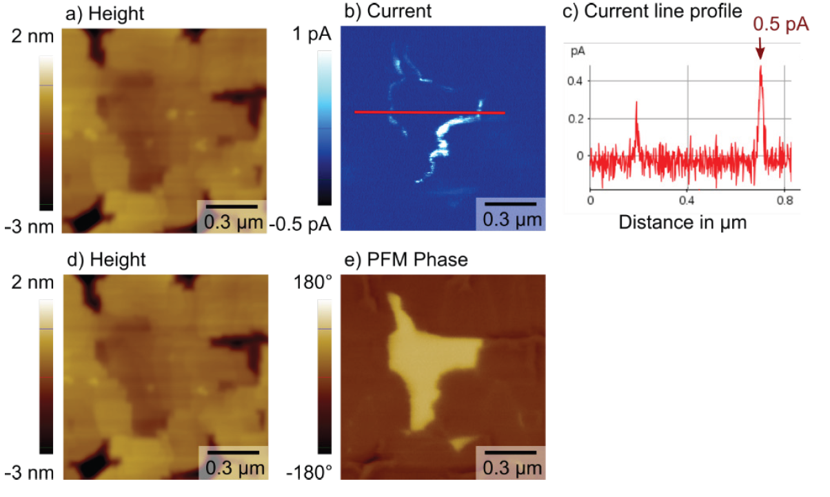
Figure 2: Results of subsequent C-AFM and PFM measurements on BFO thin film with a Park Systems NX10 AFM. a) Sample topography, b) corresponding current signal of C-AFM measurement at a DC voltage of 2.5 V and c) the line profile extracted along the red line in the current image features current maxima at the position of domain walls of up to 0.5 pA. d) Sample topography and e) corresponding PFM phase of subsequent PFM measurement detected at an AC voltage of 2 V at 355 kHz showing the contrast inversion on the oppositely polarized domain in the center of the image.
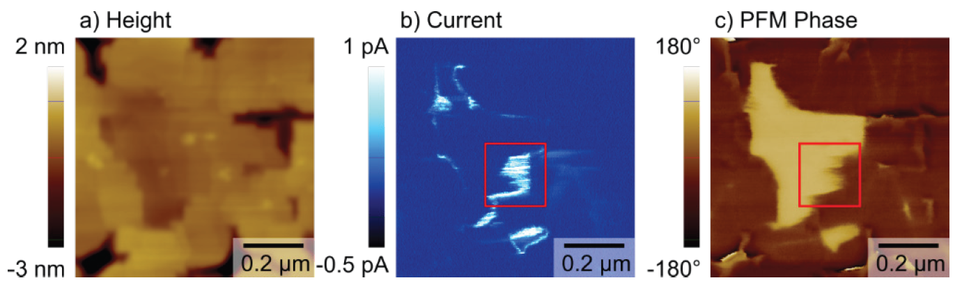
Figure 3: Results of simultaneous C-AFM and PFM measurement on BFO thin film with a Park Systems NX10 AFM, with the respective sample height in a, current signal in b and PFM phase in c at an AC voltage of 2 V at 355 kHz and a DC voltage of 2.5 V. The correlation of current and PFM phase captures the increased conductivity at the position of ferroelectric domain walls.
Following the subsequent measurements, we additionally performed simultaneous C-AFM and PFM measurements on the same domains as shown in Figure 3a-c. We again observe distinct maxima in the current signal in 3b at the position of the domain walls, resolved in the PFM phase in 3c. However, the applied DC sample voltage of 2.5 V for the current detection appeared to introduce a change in the polarization orientation of the center-domain as visible in the more blurred phase contrast in the area highlighted by the red box. Hence, for BFO thin films, which exhibit comparably low coercive fields,7 simultaneous PFM and C-AFM measurements would require even lower DC voltages.
Conclusion:
In this application note, we demonstrate that the experimental flexibility available in Park Systems AFMs facilitates a straightforward combination of C-AFM and PFM measurements without intermediate hardware changes. Therefore, Park Systems AFMs allow for a fast, accurate and reliable correlation of current detection and ferroelectric domain imaging as required to characterize conductive ferroelectric domains walls, which are promising systems for next-generation nanoelectronics.
References:
1 A. K. Tagantsev, L. E. Cross and J. Fousek, Domains in ferroic crystals and thin films, Springer, 2010, vol. 13.
2 P. S. Bednyakov, B. I. Sturman, T. Sluka, A. K. Tagantsev and P. V Yudin, npj Comput. Mater., 2018, 4, 1–11.
3 T. Sluka, A. K. Tagantsev, P. Bednyakov and N. Setter, Nat. Commun., 2013, 4, 1808.
4 J. Seidel, L. W. Martin, Q. He, Q. Zhan, Y.-H. Chu, A. Rother, M. E. Hawkridge, P. Maksymovych, P. Yu and M. ea Gajek, Nat. Mater., 2009, 8, 229–234.
5 E. Soergel, J. Phys. D Appl. Phys., 2011, 44, 464003.
6 A. Bhatnagar, A. Roy Chaudhuri, Y. Heon Kim, D. Hesse and M. Alexe, Nat. Commun., 2013, 4, 2835.
7 V. Shelke, D. Mazumdar, G. Srinivasan, A. Kumar, S. Jesse, S. Kalinin, A. Baddorf and A. Gupta, Adv. Mater., 2011, 23, 669–672.