


-
Cell temperature controller AFM GlassTemp dielectric_trench H-BN hetero_structure Mapping Composite Leakage MeltingPoint Chrome doped LateralPFM TempControl LaAlO3 Transparent PVA ThermalConductivity Sio2 BoronNitride hard_disk_media EFM VerticalPFM MESA structure epitaxy HfO2 Kevlar Gallium self_assembly Zagreb StrontiuTitanate NUS Hafnium_dioxide C_AFM Step
Report image
If you found this image unacceptable, please let us know. We will review your report and take action if we determine this image is really unacceptable.
Lithography on Si substrate
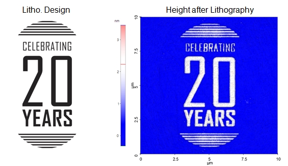
Scanning Conditions
- System: NX10
- Scan Mode: Lithography
- Cantilever: ContscPt (k=0.2N/m, f=25kHz)
- Scan Size: 10μm×10μm
- Scan Rate: 1Hz
- Pixel: 1024×512
- Litho. mode: Tip bias mode
- Litho. Tip bias: Black -10V, White 0V