


Scanning Microwave Impedance Microscopy technique for advanced electrical AFM measurements
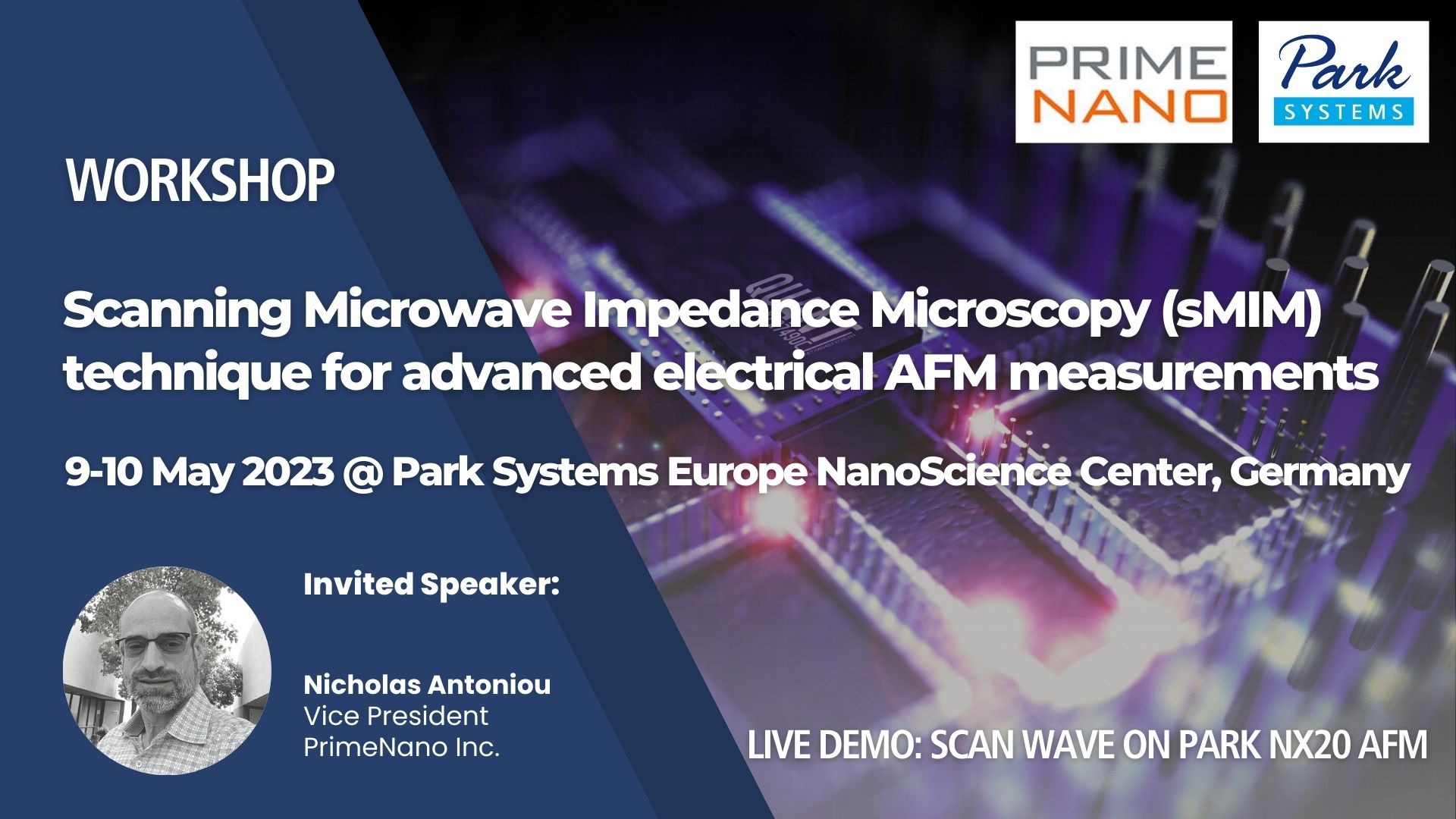
PrimeNano and Park Systems would like to invite you to learn more about Scanning Microwave Impedance Microscopy (sMIM) and how to use this technique for advanced electrical AFM measurements.
This 2-day workshop will take place on the 9th and 10th of May at the Park Systems Europe NanoScience Center in Mannheim, Germany and will be part theoretical and part hands-on sessions, which will cover a wide range of topics and applications, such as semiconductors, insulators, buried structures, nanowires, image sensors, and emerging materials.
Date: 9-10 May 2023
Time: Day 1 from 01.30 - 05.00 pm and Day 2 from 9.00 am - 01.30 pm
Venue: Park Systems Europe NanoScience Center, Schildkroetstrasse 15, 68199 Mannheim, Germany
The two-day event is free of charge and requires a registration in advance.
Deadline: 5 May 2023
________________________________________________________________________________________________________
ABSTRACT
Scanning Microwave Impedance Microscopy (sMIM) is a near-field scanning probe microscopy technique where an AFM cantilever is used as a microwave source to measure the electrical properties of materials at the nanoscale. Microwave signals are sent through an AFM cantilever and the reflected signal is collected. The reflected microwave signal is a measure of the impedance of the sample underneath the AFM tip. sMIM provides images of the variations in the local capacitance and conductance with nanoscale resolution making it an excellent method for characterizing a wide range of materials such as semiconductors, insulators, 1D/2D, ferroelectric materials and more.
________________________________________________________________________________________________________
Guest Speaker: Nicholas Antoniou
 Nicholas Antoniou holds a B.Sc. & M.Sc. in Electrical Engineering both from Texas A&M University. He has decades of experience in semiconductors and capital equipment product management. Nicholas was a member of a fab startup team and a microprocessor design startup that went IPO. After 10 years in semiconductor fabrication and design, he joined FEI Company (now ThermoFisher) where he was director for the circuit edit market. He was the principal FIB Engineer at Harvard University’s Center for Nanoscale Systems before returning to product management at Nova Measuring Instruments where he managed new materials metrology systems. He is currently VP of Product and Business Development at PrimeNano. Nicholas is an active member of IEEE, EDFAS (Electronic Device Failure Analysis Society), and ASM International.
________________________________________________________________________________________________________
PROGRAM
Please note, that the program is not yet final and will be updated on a regular basis.
Day 1
- 1.30 pm - Welcome & Coffee
- 2.00 pm - Park Systems Company Introduction
- 2.30 pm - Introducing the Park NX20 AFM
- 3.00 pm - Coffee Break & Networking
- 3.30 pm - PrimeNano Company Introduction
- 4.00 pm - Nicholas Antoniou: Introducing sMIM technique Scan Wave
- 4.30 pm - Closing Remarks
Day 2
- 9.00 am - Welcome & Coffee
- 9.30 am - Hands-on Session 1
- 11.00 am - Coffee Break & Networking
- 11.30 pm - Hands-on Session 2
- 1.00 pm - Closing Remarks
________________________________________________________________________________________________________
*Please note that this will be a live and in-person event, which will neither be streamed nor recorded.
If you have questions regarding the workshop, you can contact Katja Kiffner from Parks Systems Europe.