


CMD29 is a large international conference covering all aspects of condensed matter physics. It the 29th in the series of General conferences of the Condensed Matter Division of the European Physical Society, organized together with the Institute of Physics and will now take place from 21-26 August 2022 in Manchester. Park Systems is proud to announce its participation as an exhibitor!
- Event Dates: August 21-26
- Venue: Manchester Central Convention Complex
- Our location: booth #11

Join Dr. James Kerfoot, Applications Scientist from Park Systems UK Ltd at the CMD29 for his talk:
- ⏩ TALK TITLE: “Mapping and manipulating ferroelectric domains in parallel stacked hexagonal boron nitride with electrical AFM”
- ⏩ DATE: to come
ABSTRACT
Mapping and manipulating ferroelectric domains in parallel stacked hexagonal boron nitride with electrical AFM
Dr. James Kerfoot1
1 Park Systems UK Ltd, MediCity Nottingham, D6 Thane Rd, Nottingham, UK, NG90 6BH
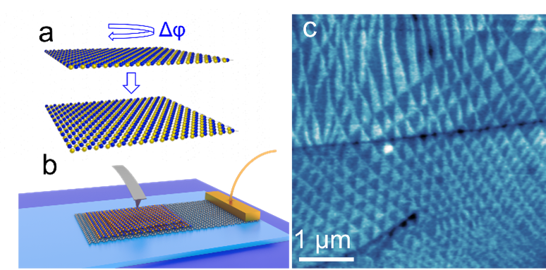
Figure: Fig. 1. Parallel stacked hBN may be formed by breaking and restacking exfoliated layers mechanically (a). Once formed, these structures may be characterised using AFM (b) in order to map the morphology of ferroelectric domains (c).
By modifying the twist angle between two crystalline materials, the registry of atoms may be modified, leading to interfacial ferroelectricity in the case of parallel stacked hexagonal boron nitride (hBN) [1-3]. We provide an account of the fabrication of such parallel stacked hBN samples using a home-built transfer setup [4] and the mapping of ferroelectric domains in these samples using both electrostatic force microscopy (EFM) and Kelvin probe force microscopy (KPFM). We address the dependence of the hBN layer thickness on the morphology of ferroelectric domains, which vary in appearance between triangular domains and more distorted irregular patterns. We then go on to discuss different ways in which such domains may be mapped and manipulated using different AFM modalities. In particular, we address the measurement of these domains with different derivatives of KPFM (both amplitude modulated and sideband KPFM inside and outside of vacuum) with higher contrast extracted for sideband KPFM. We conclude by studying the manipulation of domains both electrically by applying bias via the tip and mechanically using contact mode AFM [5].
In addition to identifying new approaches to mapping and manipulating such ferroelectric domains in layered materials heterostructures using AFM, this work is also highly relevant to new devices based upon electron tunnelling between graphene layers [6] through ferroelectric hBN, with applications both to memristive devices and tunnel diodes capable of offering increased logic per chip.
References
[1] C. R. Woods et al. Nat Commun. 12, 347 (2021).
[2] K. Yasuda et al. Science 372, 6549 1458 (2021)
[3] M. Vizner Stern et al. Science 372, 6549, 1462, (2021).
[4] Q. Zhao et al. J. Phys. Mater. 3 016001 (2020)
[5] R. Ribeiro-Palau et al. Science 361, 6403, 690 (2018)
[6] L. Britnell et al. Science 335, 6071, 947 (2012)