


Kelvin probe force microscopy (KPFM), an electrostatic force microscopy (EFM) technique, is widely applied to study electrical surface properties of various conductive or semiconductive samples. KPFM provides quantitative results of the local surface potential distribution or, if calibrated, the work function of the sample. For that, KPFM uses the same basic experimantel configuration as EFM.
The cantilever is mechanically excited while an AC voltage is applied to the tip and sample. Meanwhile, a second lock-in amplifier compensates the potential difference between sample and cantilever by applying an addtional DC bias. Thus, the feedback signal can be used to create a surface potential map. KPFM is widely used in both research and industry to image changes in work function for various applications as polymer compounds or electronic devices like solar cells.
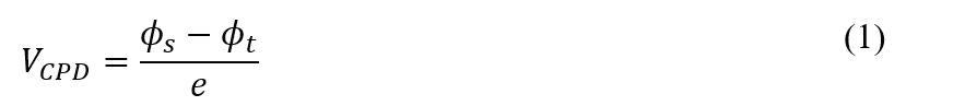
Figure 1 demonstrates the accuracy of our AM-KPFM mode on an HOGP sample with an external applied bias. The surface potential measured with AM-KPFM coincides exactly with the applied sample bias for each of the bias values (c): as the applied sample bias changed from +1 V to +2 V, to +3 V, to 0 V, to -2 V during the KPFM measurement, the detected surface potential changed accordingly to the same values.
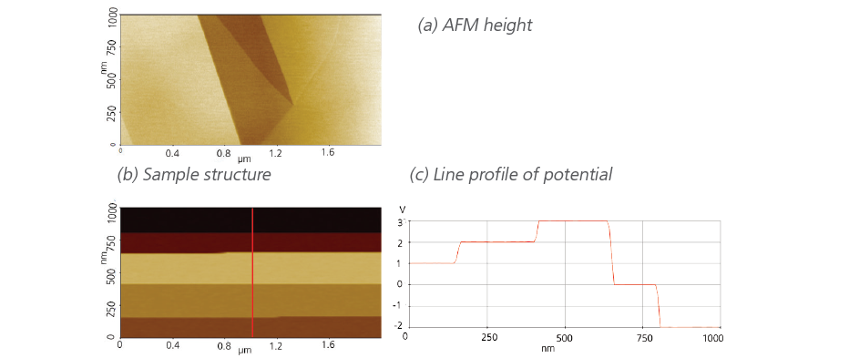
Figure 1. AM-KFPM measurend on an HOPG surface while applying stepwise a sample bias of +1 V, +2 V, +3 V, 0 V and -2 V. While the height image displays no changes depending on the applied bias (a), the KPFM channel reflects the stepwise variation in potential. The line profile extracted along the red line reproduced the applied potential in good agreement.
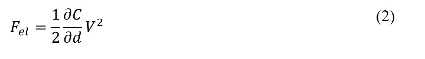
The working principle of KPFM is based on the Fermi level alignment as two conductive or semiconductive materials are brought into electrical contact as shown in figure 2. Here, one material represents the sample and the other represents the conductive AFM tip with different work functions Øs and Øt, respectively (figure 2 (a)). Once an electrical contact is established between the tip and the sample in (b), the Fermi levels of sample Efs and tip Eft align as the electrons flow from one material to the other. This Fermi level alignment leads on an offset in the vacuum levels Ev, which in turn introduces the contact potential difference VCPD between tip and sample. The VCPD is given as:
with the elemental charge e. In KPFM, VCPD is compensated at each point of the scan by applying a DC bias VDC that equals VCPD, as shown in (c).
In Park AFMs, AM-KPFM is a single-pass technique, using two different lock-ins for the topography and the KPFM signal. This has the advantage over the traditional dual-pass AM-KPFM technique that the electrical signal is measured very close to the sample surface without lifting the tip, which improves the spatial resolution and sensitivity of the surface potential.
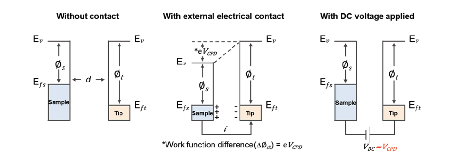
Figure 2. Energy level diagram of two materials with different work function representing the tip Øt and sample Øs. (a) Tip and sample in distance d without electrical connections, showing the offset in their Fermi levels Eft and Efs, respectively. (b) Electrical contact between tip and sample introduces Fermi level alignment via current flow i, which leads to offset in vacuum levels Ev and contact potential difference VCPD. (c) KPFM applies DC bias VDC to nullify the VCPD.
For AM-KPFM, the cantilever is mechanically excited to oscillate at its resonance frequency ω0. Amplitude changes of this oscillation due to attractive van der Waals are then used for the topography feedback, which controls the Z scanner and thereby the tip-sample distance. Park’s fast Z feedback ensures that the tip-sample distance stays in the attractive force regime to image the sample topography in True Non-contact mode. At the same time a low-frequency AC voltage ωtip (10 - 20 kHz) is applied to the tip via a second lock-in. This AC voltage leads to a modulated electrostatic interaction force Fel between tip and sample, which are viewed as capacitor:
With the capacitance C, the tip-sample distance d and the total tip-sample voltage V.
Since both AC and DC voltages are applied simultaneously between the tip and the sample, the total voltage V between the tip and the sample is expressed by the following equation:
Where VDC is the DC tip bias, VS is the surface potential on the sample and VAC and ωtip are the amplitude and frequency of the applied AC voltage, respectively. The combination of equation 2 and 3 results in three terms (a), (b) and (c) that describe the electrostatic force:
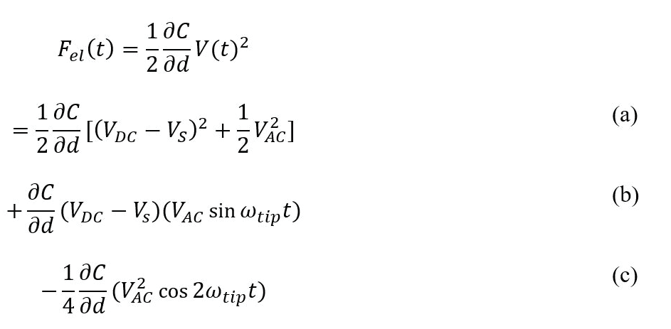
These terms can be referred to as static DC term (a), and two AC terms at ωtip (b) and 2ωtip (c). Whereas the static DC term is difficult to detect with a sufficient signal-to-noise ratio, the second lock-in amplifier used for the AC voltage in KPFM can accurately decouple the AC term at ωtip from the topography signal at ω0 to detect the electrostatic tip-sample interaction force. Since the amplitude of the cantilever oscillation at ωtip directly relates to the electrostatic force, the additional electric feedback in KPFM readjusts the DC bias to nullify this oscillation at each measurement point: for VDC=VCPD, the oscillation amplitude at ωtip becomes zero.
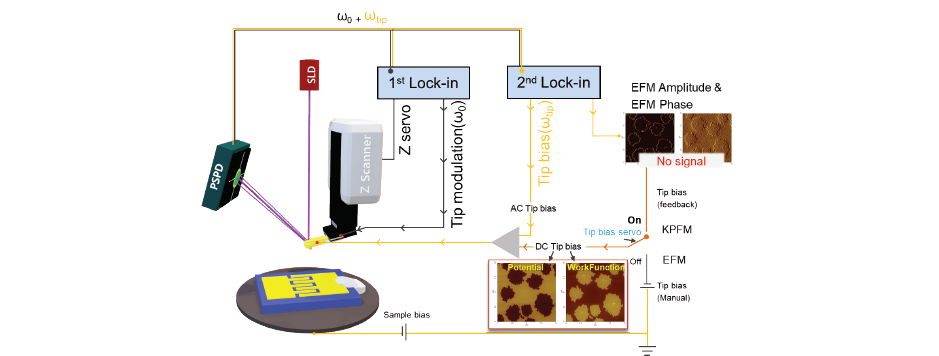
Figure 3. Schematic diagram of the experimental setup used in single-pass AM-KPFM on an exemplary electrode structure. While the first lock-in detects the sample topography measured in True Non-contact mode at the cantilever resonance ω0, the second lock-in detects the electric signal at the frequency of the applied AC tip voltage ωtip far from the resonance. The amplitude at ωtip is used in the KPFM feedback to adjust the DC tip bias to nullify the contact potential difference VCPD between tip and sample at each measurement point. From the DC bias, the surface potential image is acquired.
The variation of the DC bias at each pixel is recorded and used to quantitatively image the surface potential distribution.
Figure 3 shows a schematic diagram of the experimental setup of single-pass AM-KPFM. Two lock-in amplifiers are connected to the AFM system. The first lock-in is used for topography imaging in Park’s True Non-contact mode and the second lock-in is used for KPFM signal measurements. The second lock-in serves two purposes: The first is the application of the AC voltage with a frequency ωtip, in addition to the DC bias; the second is the separation of the measurement signal at the frequency ωtip from the cantilever oscillation at ω0 used for topography imaging.
Single-pass AM-KPFM made remarkable improvements from the traditional lift mode technique in the study of electrical properties by measuring the surface topography and potential simultaneously and eliminating topography crosstalk by using an off-resonance frequency for KPFM. However, in AM- KPFM, the measurement signal directly relates to the electrostatic tip-sample force via the amplitude at ωtip. The long interaction range of the electrostatic force leads to an averaging effect since not only the tip apex but also the cantilever itself is affected by the force. Therefore, the AM-KPFM requires a soft and short cantilever, which lowers the influence of background electrostatics from the cantilever.
AM-KPFM measurements on human hair samples are shown in figure 4, with the AFM height images in (a), (c) and the corresponding surface potential images in (b) and (d) with 15 μm by 15 μm scan size. The topography and surface potential in (a) and (b) were performed on damaged hair without treatment, while (c) and (d) show the topography and surface potential on hair treated with hair conditioner. Hair naturally has a negative charge. The KPFM signal on the damaged hair features a negative surface potential with many local variations, visible also in the line profile of the potential in (e). Many hair care scientists have been working on the development of positively charged detergents in shampoos and conditioners. Indeed, the surface potential of the treated hair is close to 0 V and more homogeneous than the damaged hair.
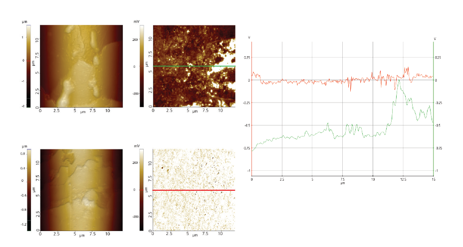
Figure 4. Single-pass AM-KPFM measurements on damaged and conditioned hair. AFM height (a) before and (c) after treatment, surface potential (b) before and (d) after treatment, line profiles (e) along the green and red lines in (b) and (d) for comparison of potential data before (green) and after (red) treatment.
KPFM can not only measure the quantitative surface potential but also absolute work functions. According equation (1), the work function of the sample Øs can be calculated from the surface potential, if the work function of the tip is known, eg: by calibration on a sample with a known work function such as gold or HOPG. In this case, Øs is given as:

After determining the work function of the tip Øs on a reference sample, a simple offset can be entered in Park’s SmartScan software and the quantitative sample work function distribution can be imaged in real time on the sample of interest.
Figure 5 shows the work function measurement on an Au surface after calibration of the tip work function using an HOPG sample. The reference work function value of an Au surface is in a range of 5.10 - 5.47 eV and the measured work function value from the single-pass AM-KPFM was about 5.27eV as shown in figure 5 (c). The work function measured on Au surfaces after calibration matched well with the known work function value of the material.
For the detection of the VCPD, there are different KPFM techniques available in Park AFMs: one is amplitude modulation KPFM (AM-KPFM) and the other is frequency modulation KPFM (FM-KPFM). Refer to the ‘Sideband KFPM mode note’ for additional information about the FM-KPFM.
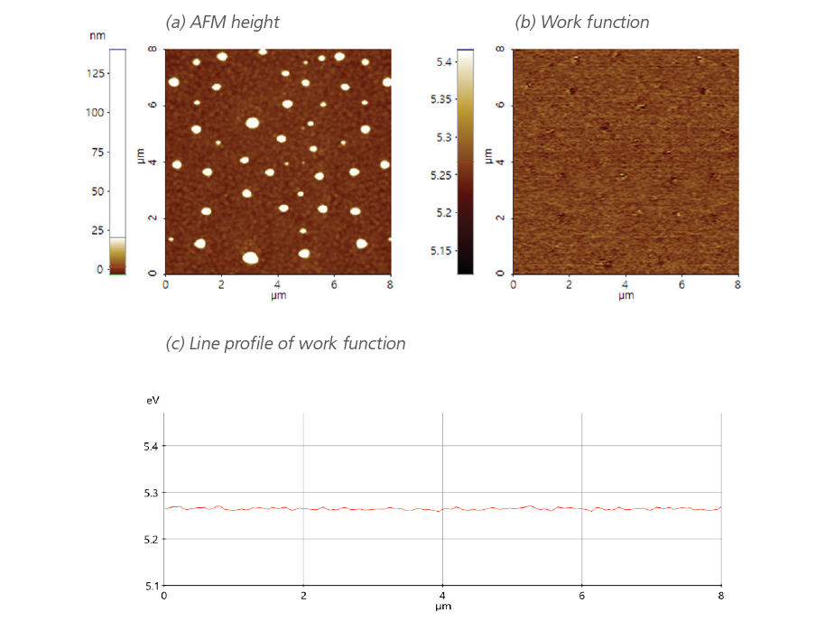
Figure 5. (a) AFM height, (b) work function image and (c) line profile of work function collected via singlepass AM-KPFM on an Au surface.