


Scanning tunneling microscopy (STM) is the oldest member in the family of scanning probe microscopy (SPM) techniques and revolutionized real-space, high resolution imaging, when it was invented in 1981 at IBM Zurich. Its impact on the scientific world was reflected, when the two inventors Gerd Binnig and Heinrich Rohrer were awarded with the Nobel prize in physics already five years later in 1986. Today, STM is widely used for high resolution imaging of conducting and semiconducting surfaces, on which the technique achieves lattice or atomic resolution. Therefore, STM is commonly applied to study surface structures and defects on the sub-nanoscale. However, STM is not suitable for insulating surfaces since the technique requires an electrical conductivity to establish a tunneling current. The high resolution of STM is achieved by probing surfaces with conducting wire that is etched to create an ultra-fine tip. Ideally, this tip consists of just a few atoms at the end. By applying a bias between the conductive tip and the conductive surface in close proximity (~10 Å), electrons begin to tunnel between tip and sample without physical contact. This tunneling current is detected by a current amplifier as the tip scans the surface (figure 1 (a)). Since the magnitude of this tunneling current strongly depends on the distance between tip and surface (figure 1 (b)), the current can serve as the feedback signal to maintain a constant tip-sample distance in the constant current mode or image the topography directly in the constant height mode.
To use STM mode on an Atomic force microscope (AFM), the system needs to be equipped with current amplifiers and probe hands for the STM wire. In Park Systems AFMs, there are three different current amplifiers available for the tunneling current measurement: the ‘internal amplifier’ and two types of ‘external amplifier’ named as VECA and ULCA (see “C-AFM mode note” for more information about current amplifiers). Each current amplifier has a different range of gain values and noise levels. For STM, amplifiers with high gain values are utilized since typical tunneling currents are below one nA.
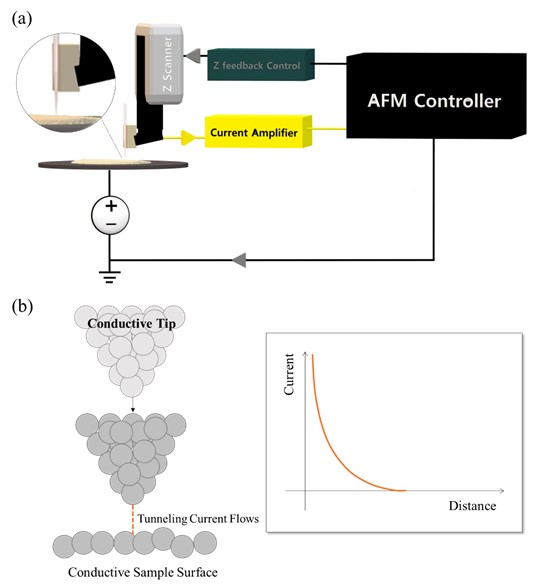
Figure 1. Schematic diagram of the experimental STM setup, including the current amplifier and the Z feedback (a).
Sketch of an STM tip with tunneling current as tip-sample distance decreases and a diagram of the corresponding distance-current graph (b).
The tunneling current It can be expressed as an exponential function of distance between tip and sample d:
where k is a constant and V is bias voltage between tip and sample. Hence, the tunneling current can change by an order of magnitude, when changing the distance between the tip and sample by only 1Å. This exponential dependence gives STM a remarkable sensitivity and enables a sub-angstrom vertical precision with a lateral resolution down to single atoms on the sample surface.
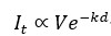
STM can be conducted in different modes: in constant height, constant current and STM spectroscopy mode. In constant height mode, the tip scans the surface at a constant Z scanner position, without height feedback. Since the tunneling current depends on the tip-sample distance, which changes with the topography, the resulting current image contains the topography information of the sample surface (figure 2 (a)). This mode should only be used on flat surfaces to avoid tip damage on protrusions in the topography or loss of current sensitivity in indentations. On the other hand, constant height STM can be operated at high scan speeds, since no height feedback is required. This allows imaging of dynamic processes.
In constant current mode, topographic images are obtained by using the tunneling current as a feedback signal for the Z scanner. As the tip scans the surface, a feedback loop compares the measured current with a default current, the so-called setpoint. If the values do not coincide, the feedback will change the Z scanner position accordingly until the setpoint current is reached. Thereby, the position of the Z scanner follows the sample topography at constant tunneling current (figure 2 (b)). Such measurements can also be conducted at different applied biases and compared to gain information on the electronic sample properties. Constant current mode is well suited to measure rough surfaces with high precision and stability, at the cost of a slower scan speed.
For STM spectroscopy, the tip-sample bias is ramped to measure current-voltage characteristics (IV curves) on specific areas or features of interest and give insights into the local electronic properties of the sample. By predefining a grid of measurement points for STM spectroscopy, a three-dimensional map of electrical properties can be obtained by measuring IV curves at each point of the grid.
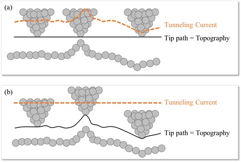
Figure 2. Comparison sketch of constant height mode (a), where the tip scans the surface at a constant Z scanner position without height feedback and the current image contains the topography information, and constant current mode (b), where the tunneling current is used as feedback signal and the Z scanner movement contains the topography information.
One example for the capability of STM measurements is shown in figure 3. Highly oriented pyrolytic graphite (HOPG) consists of several graphene layers. When two graphene layers are rotated or folded in at a certain angle, their hexagonal structures form a superlattice that is called a Moiré pattern, analogous to the macroscopic optical interference phenomenon. Electronically, the Moiré pattern can be regarded as a superperiodic interference structure of the two graphene layers. By increasing the magnification step-by-step from 2.5 µm × 2.5 µm to 500 nm × 500 nm to 200 nm × 200 nm (figure 3 (a)-(c)), the pattern could be imaged with high spatial resolution. The pattern featured a periodicity of approximately 15 nm as inferred from the line profile at the highest magnification (figure 3 (d)).
Figure 3. Moiré pattern between two graphene layers on a HOPG surface with different magnifications.
(a) displays an 2.5 µm × 2.5 µm image with a scan rate of 0.3 Hz and a resolution of 512 × 256 pixels; (b), 0.5 µm × 0.5 µm image with a scan rate of 1 Hz and a resolution of 512 × 256 pixels (c), and 0.2 µm × 0.2 µm image with a scan rate of 2 Hz and a resolution of 256 × 128 pixels. (d) Line profile of Moiré pattern extracted along the red line in (c). Zoom-in areas are indicated by yellow square box. Each image was measured with an NX10 with the STM mode, using a Pt wire as a probe. A bias of 15 mV was applied in constant current mode.