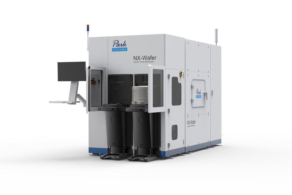
The only wafer fab AFM with automatic defect review
Low Noise, High Throughput Atomic Force Profiler
Park NX-Wafer is the industry’s leading automated AFM metrology system for
semiconductor and related fabrications. It provides wafer fab inspection and
analysis, automatic defect review for bare wafers and substrates, and CMP
profile measurements. Park NX-Wafer has the highest nanoscale surface
resolution with sub-angstrom height accuracy, scan after scan with
negligible tip to tip variation and preserved tip sharpness unmatched by
others.
Park NX-Wafer with its automated system features including auto tip
exchanger, live monitoring, target positioning without reference marks and
auto analysis makes the best semiconductor AFM tool in the industry.
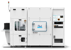
NX-Wafer
- Low noise atomic force profiler for more accurate CMP profile measurements
- Sub-Angstrom surface roughness measurements with extreme accuracy and negligible tip-to-tip variation
- Fully automated AFM solution for defect imaging and analysis
- A fully automated system with auto tip exchange, robot wafer handler
- Capable of scanning 300 mm wafers
Park NX-Wafer Operation Video
Productivity meets Accuracy
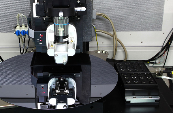
Automatic Tip Exchange (ATX)
The ATX automatically locates tips by pattern recognition and uses a novel magnetic approach to disengage a used tip and pick up a new tip, with an incredible 99.9% success rate. The laser spot is then automatically optimized along the X- and Y-axis by motorized positioning knobs.
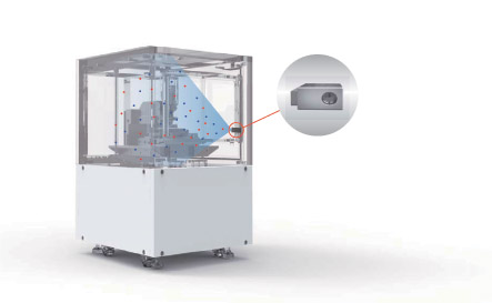
Ionization System for a more stable scanning environment
Our innovative ionization system quickly and effectively removes electrostatic charges in your sample's environment. Since the system always generates and maintains the ideal balance of positive and negative ions, it can create an extremely stable charge environment with little contamination of the surrounding area and minimal risk of accidental electrostatic charge during sample handling.
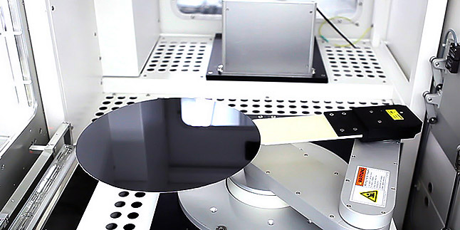
Automatic Wafer Handler (EFEM or FOUP)
The NX-WAFER can be configured for various automatic wafer handlers (EFEM or FOUP or other). The high-precision, nondestructive wafer handler robot arm fully ensures users always get fast and reliable wafer measurements.
Park NX-Wafer Specifications
System
Specification
Motorized XY stage
200mm : travels up to 300 mm × 200 mm, 0.5 µm resolution
300mm : travels up to 400 mm × 300 mm, 0.5 µm resolution
Motorized Z stage
25 mm Z travel distance,
0.08 µm resolution
Motorized Focus Stage
9 mm Z travel distance for on-axis optics
Sample Thickness Allowance
up to 20 mm
Scanner Performances
XY Scanner
100 µm × 100 µm (Large mode)
Z Scanner Range
15 µm (Large mode)
2 µm (Small mode)
AFM and XY Stage
Control Electronics
ADC
18 channels
4 high-speed ADC channels
24-bit ADCs for X,Y and Z scanner position sensor
DAC
17 channels
2 high-speed DAC channels
20-bit DACs for X,Y and Z scanner positioning
Compliances
CE
SEMI Standard S2/S8
Vibration, Acoustic Noise, and ESD Performances
Floor Vibration
< 0.5 µm/s (10 Hz to 200 Hz w/ Active Vibration Isolation System)
Acoustic Noise
>20 dB attenuation w/ Acoustic Enclosure
Facility Requirements
Room Temperature (Stand By)
10 °C ~ 40 °C
Room Temperature (Operating)
18 °C ~ 24 °C
Humidity
30% to 60% (not condensing)
Floor Vibration Level
VC-D (6µm/sec)
Acoustic Noise
Below 65 dB
Pneumatics
Vacuum : -80 kPa
CDA (or N2): 0.7 MPa
Power Supply Rating
208V - 240 V, single phase, 15 A (max)
Total Power Consumption
2 KW (typical)
Ground Resistance
Below 100 ohms
Options
Long Range Sliding Stage
• 200mm : 10 mm (optional 25 mm)
• 300mm : 25 mm (optional 10 mm or 50 mm)
Automatic Tip Exchange (ATX)
Automatic Tip Exchange performs fully automated tip exchanges in order to seamlessly continue automated measurement routines. It automatically calibrates cantilever location and optimizes measurement settings based on measurements of a reference pattern. Our novel magnetic approach to the tip exchange yields a 99% success rate, higher than the traditional vacuum techniques.
Automatic Wafer Handler (EFEM or FOUP)
The XE-3DM can be further customized by adding an automatic wafer handler (EFEM or FOUP or other). The high-precision, nondestructive wafer handler robot arm fully ensures XE-3DM users to receive fast and reliable wafer measurement automation.
Ionization System
Ionization system effectively removes electrostatic charges. It ionizes the charged objects and is very reliable since the system always generates and maintains an ideal balance of positive and negative ions without causing any contamination to the surrounding area. It also reduces the accidental electrostatic built-in charge that may occur during sample handling.
Dimensions & Weight
200 mm System
2732 mm(w) × 1100 mm(d) x 2400 mm(h)
w/ EFEM, 2110 kg approx. (incl. Control Cabinet)
Ceiling Height
3000 mm or more
Operator Working Space
3300 mm (w) x 1950 mm (d), Minimum
300 mm System
3486 mm(w) × 1450 mm(d) x 2400 mm(h)
w/ EFEM, 2950 kg approx. (incl. Control Cabinet)
Ceiling Height
3000 mm or more
Operator Working Space
4770 mm (w) x 3050 mm (d), Minimum
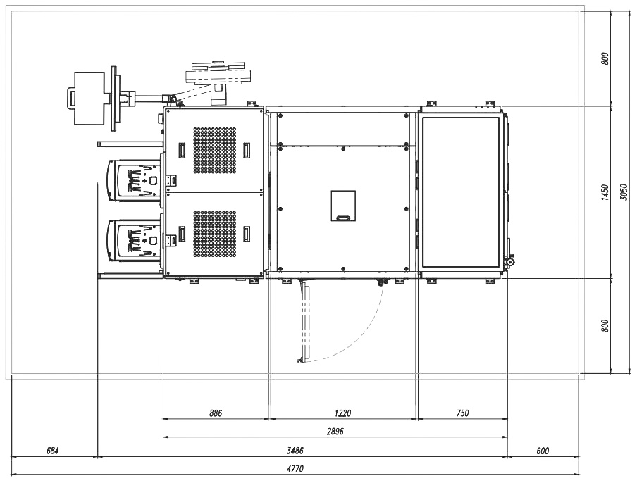 [ Park NX-Wafer 300mm installation layout ]
The only wafer fab AFM with automatic defect review
Low Noise, High Throughput Atomic Force Profiler
Park NX-Wafer is the industry’s leading automated AFM metrology system for semiconductor and related fabrications. It provides wafer fab inspection and analysis, automatic defect review for bare wafers and substrates, and CMP profile measurements. Park NX-Wafer has the highest nanoscale surface resolution with sub-angstrom height accuracy, scan after scan with negligible tip to tip variation and preserved tip sharpness unmatched by others.
Park NX-Wafer with its automated system features including auto tip exchanger, live monitoring, target positioning without reference marks and auto analysis makes the best semiconductor AFM tool in the industry.
- Low noise atomic force profiler for more accurate CMP profile measurements
- Sub-Angstrom surface roughness measurements with extreme accuracy and negligible tip-to-tip variation
- Fully automated AFM solution for defect imaging and analysis
- A fully automated system with auto tip exchange, robot wafer handler
- Capable of scanning 300 mm wafers