


Automated Non-Destructive Imaging and Characterization of Graphene/hBN Moiré Pattern with Non-Contact Mode AFM
By Dr. Ardavan Zandiatashbar, Ph.D.,
Park Systems Inc., Santa Clara, California.
INTRODUCTION
Graphene has attracted researchers' attention due to its unique band gap structure, which allows it to be used in high-mobility semiconductor devices. However, realization of such a graphene-based high-performance device has been challenging due to lack of a suitable substrate. This challenge has been recently addressed by the development of epitaxial growth of graphene on hexagonal boron nitride (hBN)[1, 2].hBN is a suitable substrate for graphene due to its highly similar hexagonal patterns. A moiré pattern is the superlattice generated as the result of a ~2% mismatch between graphene and hBN lattices, with periodicity values larger than each of the two materials’ lattice constants by two orders of magnitude[3].
Scanning probe microscopy (SPM) is a key technique for characterization of moiré pattern. This is due to the fact that SPM can provide the highest Z resolution compared to any other microscopy technique[4].Therefore it is essential to verify successful fabrication of graphene/hBN devices by epitaxial growth methods; however, SPM has been challenging for two major reasons: perplexing parameter optimization with a steep learning curve for new researchers (and even experts), as well as the high cost of specialized tips for highresolution imaging. In addition, frictional mode SPM involves mechanical tip-sample engagement, making it a destructive method for characterizing the graphene/ hBN devices. Almost all research performed on characterization of the moiré pattern uses destructive SPM modes [1, 2, 3] Non-contact mode atomic force microscopy (AFM) is a non-destructive SPM technique availablesince the late 80s [5].In order to perform non-contact mode imaging, tipsample separation must be controlled accurately. This was challenging, and it was one of the limitations of this technique at the beginning. However, thanks to research and development, the technique has reached maturity over the past decade and is now provided as the standard AFM imaging mode by Park Systems.
In this article, the need for easy, nondestructive SPM characterization of moiré pattern has been addressed by the automated non-contact mode AFM imaging technique developed by Park Systems. The commercial name of the product is SmartScan™ Auto Mode. Until today, SPM characterization of moiré pattern has been challenging, expensive, destructive, and time consuming. Now, with this new solution researchers can easily and reliably perform quality control of the fabricated graphene-based devices.
MATERIALS AND METHODS Non-contact mode AFM imaging
Non-contact mode imaging is performed by modulating the cantilever’s oscillation amplitude at a frequency slightly higher than the resonance frequency of the cantilever in air (far from the sample surface). As the tip approaches the sample surface, tip-sample interaction enters into the attractive state. Non-contact mode imaging is performed when tip-sample interaction is in the attractive state. The cantilever oscillation phase is negative in the attractive state and positive in the repulsive state. By further decreasing tip-sample separation, the interaction switches to the repulsive state (dynamic or tapping mode). Variation of amplitude as a function of tipsample separation is shown in Figure 1and is hereafter referred to as the “A-d curve”. As the oscillating cantilever approaches the sample, oscillation amplitude decreases due to tipsample interaction forces. However, as the tip descends, cantilever amplitude has a small sudden increase in value. The slight jump in amplitude is associated with changing sign of phase from negative to positive. This indicates that tip-sample interaction switches from the attractive to the repulsive state. In other words, the cantilever switches from non-contact mode to tapping mode. As the tip continues approaching the surface, the amplitude value approaches zero. Now, if the cantilever is lifted and tip-sample separation increases, the jump from the repulsive to the attractive stateoccurs again, but at a greater distance from the sample surface. If imaging is performed with cantilever oscillation amplitudes larger (smaller) than the second (first) jump point, imaging is performed in non-contact (tapping) mode, and tip-sample interaction is maintained in the attractive(repulsive) state. If imaging is performed with amplitude values between the first and second jump, the tip-sample interaction will be unstable and switch between the attractive and repulsive states, which is undesirable for imaging purposes[6]. In these conditions, the feedback system becomes bistable.
SmartScan™ Auto Mode
SmartScan™ is the new operating software developed by Park Systems for operating research AFM systems. Auto Mode is one of the major innovations provided by SmartScan™ and is used for performing measurements. Itessentially has two automationsteps after placing the tip and sample: positioningand imaging. In the positioning step, the location of sample surface is found by detecting tipsample van der Waals (VdW) interactions. In this step, the tip approaches the sample at a rate of 0.5mm/sec to find the sample surface. Although this is a fairly rapid approach speed, the tip does not come into physical contact with the sample surface. Instead, thetip-sample attractive state and its effect on cantilever oscillation amplitudeare used to detect the sample surface. As a result, tip sharpness and the original state of the sample surfaceare preserved. After detecting the surface, the tip is lifted to a safe distance (about 200 μm)to allow navigating the sample surface and locating the area of interest via optical microscope. Since the location of the sample surface is known, the optical microscope is brought into focus automatically.
After locating the area of interest, theimaging stepbegins. During the imaging, oscillation frequency, free air and setpoint amplitudes, feedback control parameters, and scan rate are optimized automaticallyaccording to desired image quality.The user only needs to specify scan size, number of scan lines, and desired image quality. As described above, it is important to maintain accurate tip-sample separation to maintain tip-sample interaction in the attractive state. Accurate tip-sample separation is determined by SmartScan™ Auto Mode based on the A-d curves shown in Figure 1.
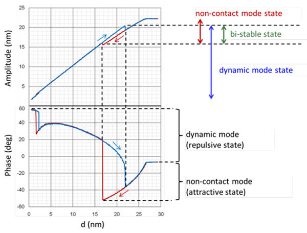
Figure 1. AFM cantilever oscillation amplitude (upper) and phase (lower) vs. tip-sample separation (d) known as the A-d curve for constant Z actuator driving power. The red curves denote the tip approaching the sample and the blue curvs show the response when the tip is retracted from the sample surface. (Image used with permission from Nanoscientific)[7]
Graphene epitaxy on hBN
For this study, hBN samples were prepared by mechanical cleavage of BN crystals on a silicon substrate with a 300 nm SiO2 epilayer. Graphene was grown by CVD epitaxial growth. Additional information can be found in the work by Yang et al.[1]
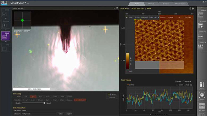
Figure 2. The newly developed SmartScan™ Auto Mode which allows automated sample surface detection and imaging with minimal user interaction. On the left the major buttons including “positioning” and “image” are shown. Screenshot was taken while the software was collecting a 150 nm image of graphene/hBN sample in Non-Contact mode. User only needs to select scan size, image resolution, and quality/speed.
RESULTS
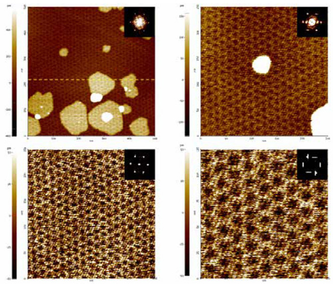
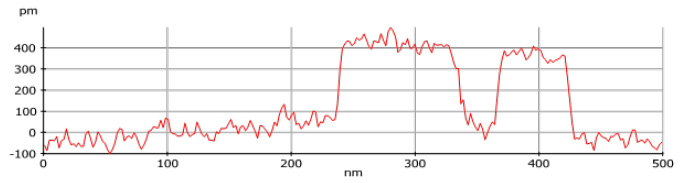
The graphene/hBN samples were imaged usinga standardnon-contact mode silicon AFM probe with a nominal tip radius of 7 nm and force constant of 42 N/m. The tip resonance frequency was selected at 316 KHz by the software. The sample surface was detected by automated software and followed by navigating the sample via optical microscopy and automated imaging. The images were collected in 500nm, 250nm, and 125nm square sizes. First, lower magnification images were collected, and thenimage size was decreased for higher magnifications. Non-contact mode AFM images of the graphene/hBN samples are shown in Figure 2.a. The moiré superlattice of epitaxial graphene is easily distinguishable in all images in the form of a hexagonal pattern. The hexagonal pattern was evaluated and confirmed by fast Fourier transform (FFT) of AFM images,illustrated in the insets of Figure 2.a. Additional grains of the secondary layer can be observed in the 500nm image. To characterize the height of the secondary grains, a line profile of the 500 nm image was selected as illustrated in Figure 2.b. The height of the secondary grain is ~3.8Å. The moiré pattern is observable on the secondary grains, as well.
DISCUSSION
The moiré superlattice is characterized in Figure 3 by using one of the 250 nm images.A FFT filter is applied to eliminate additional signal and enable easier characterization of the pattern. The lattice constant of the moiré pattern is measured to be ~15 nm. This is consistent with the simulation results of ~14nm, which is two orders of magnitude larger than lattice constants of graphene and hBN[3].The red and green lines indicate the axes of the superlattice and are used for measuring periodicity in either direction. The peak-to-valley value for each line is below 0.7Å. The continuity of moiré pattern over all the spaces indicates successful growth of epitaxial graphene over hBN. It also indicates growth of graphene on hBNirrespective of the number of layers, as seen in the 500 nm image in Figure 2. The formation of the moiré pattern is the result of a ~2% mismatch between the lattice constants of graphene and hBN.
To the knowledge of the authors, imaging the moiré pattern of epitaxial graphene in non-contact mode has not until now been performed. This is of great importance, since the samples are fragile (low friction between graphene and hBN). Therefore, minimized interaction between the tip and sample is desired to maintain the conditions of the sample during the characterization.There is no mechanical interaction, and the imaging is performed in the ambient atmosphere without the need for a vacuum. Therefore,noncontact mode imaging, as a benign characterization technique, plays a key role for characterization of devices fabricated by epitaxial growth of graphene on hBN or other two-dimensional materials. Preserving tip sharpness is also another advantage of using non-contact mode imaging. In addition to reducing the tip cost, a reliably sharp tip preserves the image quality and improves measurement repeatability. Although finding correct tip-sample distance for true non-contact mode imaging is challenging and could depend heavily on user experience, using automated software enables performing the measurements with minimal user interaction. It also improves repeatability, productivity, and measurement throughput. A standard non-contact mode probe (PPP-NCHR) was used for this measurement, not the special or super-sharp tip usually required for this sort of high resolution imaging. In non-contact mode, VdW interaction between tip and sample is utilized to image the moiré superlattice with high resolution and repeatability. Note the moiré pattern lattice constant (15nm) is almost twice the nominal tip radius (7 nm). This enables decreasing the characterization cost for potential devices fabricated based on epitaxial graphene.
CONCLUSION
The moiré superlattice of epitaxial graphene grown on hBN has been imaged in noncontact mode using a recently developed automated AFM. Images were collected using a standard silicon probe with nominal tip radius of 7nm. The moiré superlattice was characterized, and the lattice constant of ~15 nm was verified against simulation values. The newly developed automated AFM enables minimal user experience needed for performing this type of high-resolution measurement. It also improves repeatability, productivity, and throughput. Automated non-contact mode imaging is therefore an efficient characterization technique for quality control of devices fabricated by epitaxial growth, such as graphene/hBN-based devices.
ACKNOWLEDGEMENT
The authors are immensely grateful to David Goldhaber-Gordon and Patrick Gallagher from Stanford University and Guangyu Zhang from Chinese Academy of Sciencesfor providing the graphene/hBN sample and fruitful discussions.
 a)
a)
 b)
b)
Figure 3. a) Non-contact mode images of graphene-hBN samples with 500 nm, 250 nm, and 125 nm scan sizes. No filter has been applied to the images. The insets indicate Fourier transformation of the image. b) The profile of the dashed line in the 500nm image.
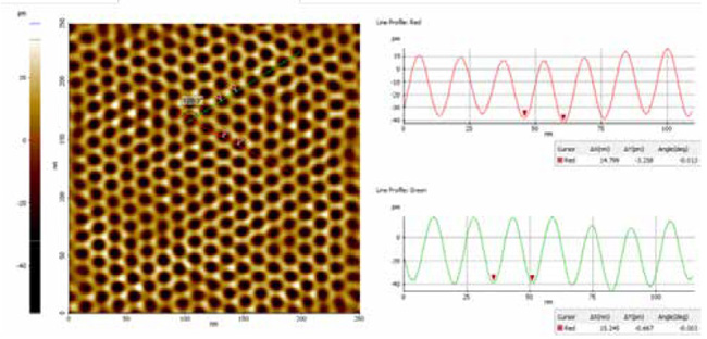
Figure 4. A FFT filter is applied to one of the 250nm images in Fig. 2.a. to characterize the moiré superlattice. Line profiles for the red and green lines are shown on the right side.
REFERENCES
1. W. Yang, G. Chen, Z. Shi, C.-C. Liu, L. Zhang, G. Xie, M. Cheng, D. Wang, R. Yang, D. Shi, K. Watanabe, T. Taniguchi, Y. Yao, Y. Zhang and G. Zhang, "Epitaxial growth of single-domain graphene on hexagonal boron nitride," Nature Materials, vol. 12, pp. 792-797, 2013.
2. S. Tang, H. Wang, Y. Zhang, A. Li, H. Xie, X. Liu, L. Liu, T. Li, F. Huang, X. Xie and M. Jiang, "Precisely aligned graphene grown on hexagonal boron nitride by catalyst free chemical vapor deposition," Scientific Reports, vol. 3, no. 2666, 2013.
3. C. R. Woods, L. Britnell, A. Eckmann, R. S. Ma, J. C. Lu, H. M. Guo, X. Lin, G. L. Yu, Y. Cao, R. V. Gorbachev, A. V. Kretinin, J. Park, L. A. Ponomarenko, M. I. Katsnelson, Y. N. Gornostyrev, K. Watanabe, T. Taniguchi, C. Casiraghi, H.-J. Gao, A. K. Geim and K. S. Novoselov, "Commensurate–incommensurate transition in graphene on hexagonal boron nitride," Nature Physics, vol. 10, pp. 451-456, 2014.
4. G. T. Smith, Industrial Metrology: Surfaces and Roundess, Springer, 2002.
5. G. Binnig, C. F. Quate and C. Gerber, "Atomic Force Microscope," Physical Review Letters, pp. 930-933, 1986.
6. R. Garcia and R. Perez, "Dynamic atomic force microscopy methods," Surface Science Reports, pp. 197-301, 2002.
7. A. Zandiatashbar, "Sub-angstrom roughness repeatability with tip-to-tip correlation," NanoScientific, no. Winter, pp. 14-16, 2014.